 Hulk
HulkThe UNL2003 IC contains 7 High Voltage, High Current NPN Darlington Transistor Arrays each rated at 50V, 500mA in a 16-pin DIP package. You can connect the IC directly to a digital logic (like Arduino or Raspberry Pi, TTL or 5V CMOS device) without an external dropping resistor. This IC features "common-cathode flyback diodes" for switching inductive loads. The ULN2003 is known for its high current and high voltage capacity. The Darlington pairs can be "paralleled" for higher current Output. The inputs are capable with TTL and 5v CMOS logic. Now, let's deep-dive and check out the internals of the IC and how it can be used in our projects.
Pin Configuration and Functions

The notch on the top indicates the starting and stopping points of the numberings of the chip. Starting from left to right going counterclockwise this is the Pin number 1 of the IC. * On the left hand side Pin 1 to 7 are the Base Inputs.
* On the right hand side Pin 10 to 16 are the Collector Outputs.
* Pin 9 is the Common Cathode node for flyback diodes (required for inductive loads).
* And, Pin 8 is the Common Emitter shared by all channels of the IC. This pin is typically tied to ground.
Detailed Description

Inside the IC is the arrays of the 7 NPN "Darlington Transistors". Darlington Transistors were first invented in 1953 by Sidney Darlington. A Darlington pair is a circuit consisting of two Bipolar Transistors with the Emitter of one transistor connected to the Base of the other transistor. In this setup, the current amplified by the first transistor is further amplified by the second transistor. The collectors of both transistors are connected together. This configuration has a much higher current gain than each transistor taken separately. A small base current can make the pair switch to a much higher current.

It appears as if it is just a single transistor, with only one base, one collector, and one emitter. Creating a high current gain approximately to the product of the gains of the two transistors:
β Darlington = (β 1 * β 2) + β 1 + β 2
Since, β1 and β2 are high enough, we can write the above statement as:
β Darlington ≈ β 1 * β 2
This connection creates the effect of a single transistor with a very high-current gain.

The 7 outputs are all "Open Collector".
By Open Collector, we mean a collector that is not attached to anything. It's just open.
In order for an open collector output device to work, the open collector has to receive sufficient power.
In order for an NPN transistor to work, the collector and the base both need to receive sufficient power. The base turns the transistor on, and then a much greater current flows from collector to emitter, but only if the collector has sufficient positive voltage.
So if you want to connect a load to the Output of the chip with an open-collector-output, you must attach the load to a positive voltage source that is sufficient enough to drive the load. Hence, the +ve side of the load connects to the +ve voltage rail and the -ve side connects to the OUTPUT pin of the IC.
Hence, when the Base current goes HIGH, the current flows from the collector to emitter and the Output logic goes LOW turning ON the LED (load) connected to the OUT pin of the IC and vice-versa.
The maximum Output Current of a single OUTPUT pin is 500mA and the total emitter-terminal current is 2.5A as per the datasheet.

Now, let's have a closer look at a single Darlington pair (internal circuit diagram) of the ULN2003 IC. The GPIO input voltage is converted to base current through a series base 2.7kΩ resistor connected between the Input and Base of the Darlington NPN junction. This allows the IC to connect directly to a digital logic (like Arduino, Raspberry Pi, TTL or 5V CMOS device) without the need of external dropping resistors operating at supply voltages of 5V or 3.3V. The 7.2kΩ and the 3kΩ resistors connected...
Read more »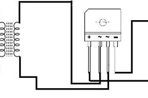
 kamalkedin123
 Electroniclovers123
 utsourceproduct