Marius Popescu
Introduction
Thermal Imaging technology used to be priced prohibitively outside the budget of hobbyists until recent years. Late 2012 when I started working on my 1st Thermal Imaging project, the lowest cost thermal camera available on the market was the Flir i3 (priced at $995 back then). Moreover, there was (to my knowledge) absolutely no lower cost, open-source alternative solution on the market to these expensive, proprietary devices - that mostly had to do with the high development and manufacturing costs of high/medium performance IR FPAs and lenses and with the timid availability of low cost, low performance IR modules (FPA + lens + ASIC), still not implemented in any low-cost Thermal Imager.
I was therefore highly motivated to explore the possibility of developing a Thermal Imaging platform that was low cost ( < $200 to manufacture) and could offer sufficient performance for some of the less demanding hobbyist level tasks. That's how I've started working on Thermal Imaging devices.
A bit of background
1st attempt: Mechanically Microscanned Thermal Imager (MMTI)
I've started prototyping a device around the MLX90620BAD 16x4 IR array. The idea was to select a low-cost (implicitly low performance) IR FPA that had a low pixel FOV (2.5° x 2.6° FOV / pixel) and a satisfactory NETD (0.08°K at 1 fps in its datasheet; found out the hard way during testing that it was more like 0.4-0.5°K - still have no clue how they got to that figure).
Then, by means of a stepper-motor controlled pan-tilt platform (that had its rotation axes centered as well as possible to the FPA's surface center in order to simplify pixel position calculations) produce a pattern of controlled sub-pixel shifts (microscanning) of the whole IR module.
Each thermal data frame would be sequentially fed via WiFi to a connected iOS device that would form in realtime a composite high resolution image from the individual low-res frames (in the end a 176 x 44 final high resolution image would be obtained out of 121 frames of 16x4).
The prototype consisted of:
- Melexis MLX90620BAD 16x4 IR array
- PIC32MX795F512L based USB Starter Kit II + Starter Kit I/O Expansion Board
- MRF24WG0MA Wi-Fi G PICtail Daughter Board
- 3-axis stepper control board based on 3 x A3977SED (self designed / manufactured board that I had lying around since my early 20's) - naturally, only 2 axis used
- Vexta PK246PA stepper motors that I had lying around (1.8° / step - had to use 1/8 micro stepping to obtain 0.225° steps to fulfill my sub-pixel shifting resolution demands)
- 3S 1600mAh LiPo battery
- cheap laser module (from a laser pointer) - to evaluate microscanning pattern accuracy and orientation
- custom pan-tilt platform (self designed / CNC manufactured) - to allow precise centering of MLX90620BAD FPA surface center to the pan-tilt platform rotation axes
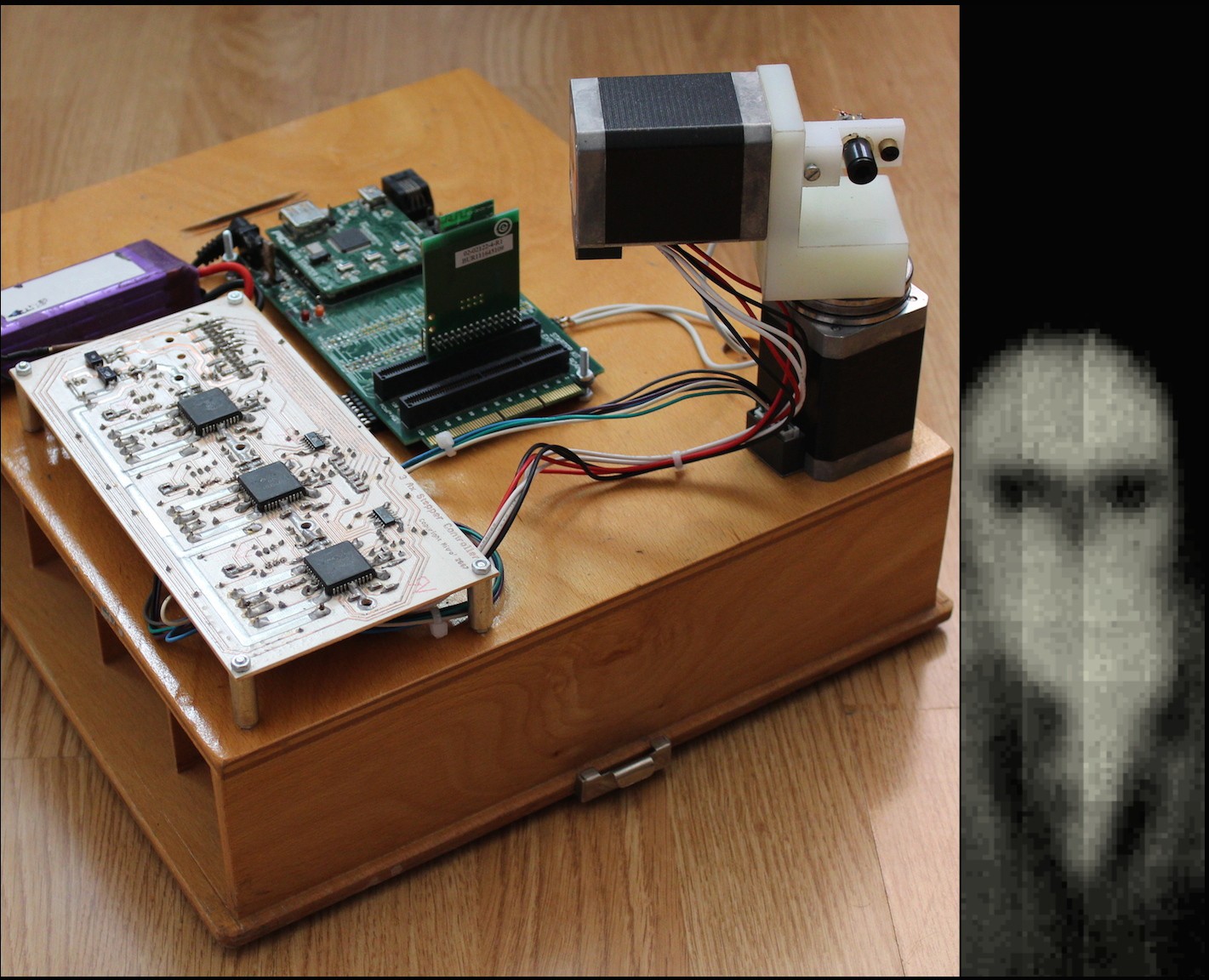
Here's an image of what the Hardware Prototype of MMTI looked like and to the right is the high-res composite image 176 x 44 (formed out of 121 frames of 16x4) - 'self portrait' - yes, I stood frozen for 121 seconds :)
Conclusions drawn from the MMTI prototype testing:
- Successfully verified the validity of the microscanning concept of this particular setup - I was actually surprised by the rather good alignment of pixels and frames
- Sufficient spatial resolution
- Much higher NETD than expected (specified 0.08°K at 1 fps in MLX90620BAD datasheet; found out the hard way during testing that it was more like 0.4-0.5°K - still have no clue how they got to that figure)
- High pixel non-uniformity (although all MLX90620 are factory calibrated to a certain degree of non-uniformity); I had to implement a pre-scan calibration to get to satisfactory uniformity
- High measurement noise for MLX90620BAD (as sensor frame rate is increased, the noise increase too, rendering any frame rate higher than 4 FPS useless for this application)
- Concluded that the primary performance limiting factors of the system were:
- the high NETD of MLX90620BAD (measured 0.4-0.5°K) -> a sensor with a lower NETD could greatly improve the thermal details of captured images
- high pixel non-uniformity -> a sensor with better pixel non-uniformity would improve the image overall quality and need no pre-scan calibration
- high measurement noise -> a sensor with lower measurement noise would improve the visible thermal details and overall image quality
Search for IR array module alternatives
At this point, I've decided that a new IR array that exhibits better characteristics in the areas that MLX90620BAD lacks (NETD, pixel uniformity, measurement noise) is needed.
I've selected the Omron D6T-44L-06 (4x4 pixels) for testing and adapted it for mounting on the previously developed MTTI prototype.
The following conclusions have been drawn after evaluating D6T-44L-06:
- it exhibits much lower measured NETD (specified at 0.14°K; actual measured temperature resolution is 0.1°C)
- better pixel uniformity
- much lower measurement noise
- however, its lower optical resolution (4x4) and pixel FOV are significantly worse (no surprise here)
- due to a sum of factors such as low optical resolution, high pixel FOV, inaccurate alignment of sensor to pan-tilt platform (tried simply adapting the sensor holder custom designed to align the MLX90620 to hold a modified D6T-44L-06 module PCB) I was unable to produce usable composite images with this sensor :(
Nevertheless, if only a higher resolution D6T module existed and exhibited the same characteristics that I liked about D6T-44L-06... I knew from prior Omron material that a 16x16 sensor was in development and not too surprisingly in May 2013 it was announced. However, it's estimated to be commercially available only late 2014.
In the meantime, I had to find an alternative FPA so I don't get bored!
In past I've planned to use a Panasonic Grid-EYE (8x8 pixels) IR array but was deterred by the public unavailability of a complete datasheet and by my unanswered requests for a data sheet that I've sent to Panasonic.
To my surprise, at some point I've discovered there's a breakout board available for the AMG88xx (Grid-EYE) sold and sponsored by Digikey and the company that designed it posted a full datasheet on their eewiki page. Later, Panasonic also had another version of the full datasheet posted on their product page but they seem to have removed it afterwards?!
The Panasonic Grid-EYE infrared array seemed to be an interesting little sensor (highly compact, low cost, decent theoretical performance).
Sourcing an AMG88xx in Europe was a challenge in itself due to export regulation (Dual-use technology... although I find it hard to imagine how such low resolution/low FPS sensor could be used in any military application).
Eventually I was able to get hold of an AMG8832 for evaluation.
Several conclusions after evaluating AMG8832 performance:
- good thermal resolution (0.25°K as specified) but worse than D6T-44L
- better pixel uniformity than MLX90620 but worse than D6T-44L
- lower measurement noise than MLX90620 (at similar framerate) but worse than D6T-44L
Seems that Omron D6T-1616L is still my best choice (judging by its predecessor's - D6T-44L - performance and by D6T-1616L specs.), but until it becomes commercially available the AMG8832 is the second best thing.
- Later this week I will post more comparison data between the 3 sensors that I have been testing (videos, measured parameters etc.)
To be mentioned is that while in contact with Omron I was offered the possibility of evaluating an Engineering Sample of the unreleased D6T-1616L (16 x 16) in August 2014.
So the Omron D6T-1616L (16 x 16) will be used in the TJ Gen1 prototype currently in the works!
What others have been doing meantime
Meanwhile I've also took note of the highly successful IR-Blue Kickstarter campaign and felt excited that low-cost open-source thermal imaging seems to start taking off. I've found it inspiring and further motivated me to push forward with this.
Yeah, there was also this Mu Thermal Camera campaign that not really surprisingly turned out to be vaporware but I must admit it really got me intrigued me at first.
What really made me shift the focus of my work was the announcement of Flir One in early 2014. At $350 with a FPA of 80 x 60 (Flir Lepton), finally Thermal Imaging was getting more affordable. Still proprietary though :(
It kind of rendered my envisioned MMTI useless at its intended $200 production costs. But all for the better, as Thermal Imaging just became considerably more affordable and as a side effect it forced other major FPA manufacturers to hop the wagon and be competitive in that price range.
2nd attempt: TJ (Thermal Jack) Gen0 Prototype
The IR-Blue was getting it (the open-source Thermal Imaging), but in terms of performance and cost ($160 - $195) it was still not there yet. So I thought I might be able to do better.
I was immensely inspired by the HiJack Project - they brought the idea of connecting a low-power sensor system to a smartphone / tablet headphones jack with the purpose of drawing power and communicating through it. They've designed and implemented an open-hardware / open-source prototype which later even became a dev kit manufactured by Seeedstudio.
The idea is especially exciting from the perspective that it's a royalty-free 'App Store-friendly' solution of physically interfacing to iOS devices (instead of joining Apple's costly MFi Program). Square also seems to agree - maybe they were the ones that inspired the HiJack guys?
Even better it's much simpler and less expensive than Bluetooth Low Energy (another non-MFi way of interfacing to iOS devices) and requires no external power.
So here's a crazy idea:
Why not have an FPA + micro controller directly connected to the smartphone's / tablet's headphones jack? And so the work on TJ begins... :)
Harvesting power from the headphones jack
Harvesting power from the headphones jack is not a trivial feat. The smartphone / tablet is not able to simply output a DC voltage level on the audio channels (the audio channels are AC coupled for protection) so the best next thing that you can get is a high frequency Sine Wave (up to almost 22 Khz). What makes things more difficult is the amplitude of the generated sine wave which, when in load, is so low that it's hardly useful for rectification + step-down / step-up.
The solution that the Hijack project hardware came up with was to boost the sine wave up using a micro-transformer and then rectify it with a FET bridge to minimize voltage drops during rectification and feed through an LDO regulator to power the digital circuitry.
I found the HiJack power harvesting solution a bit too complex for the needs and I thought that I might be able to reduce complexity and cost. Why not use a simple schottky-based Cockroft-Walton multiplier and simply feed the multiplied DC voltage into an LDO regulator? Let's try that!
A 2-stage Cockroft-Walton multiplier + 3.3V LDO seemed to work really well providing the estimated ~5.5mA @ 3.3V needed to power the FPA and the micro controller. I mean, it worked flawlessly on the devices that I had around for testing at that time (iPad 3, iPhone 4). That until I've tried connecting it to an iPhone 5s which blew up (I'm kidding! :P). It just didn't work because the amplitude of the sine-wave generated by the iPhone 5s was almost half of the one of iPad 3 / iPhone 4.
Back to the drawing board. I've tried several improvements as increasing number of multiplier stages, increasing capacitor values, trying a full-wave configuration, all in the effort of getting the output voltage to acceptable levels and reducing ripple.
Meantime, NXP Quick-Jack comes to the rescue! Quick-Jack is a redesign of the HiJack hardware coming from NXP. The Quick-Jack designers seem to also have thought that the Hijack power-harvesting circuit was overcomplicated and not surprisingly they also came up with a simple voltage multiplier except with a slightly different topology - the well-known Dickson charge pump.
So, why don't I try that too?
I ended up using a 5-stage Dickson charge pump + a 3.3V LDO regulator which was able to generate the ~5.5mA @ 3.3V that I needed, even on the iPhone 5s! Success at last.
- Although I must admit I had to use a small trick: I've connected the audio channels in parallel. So, that means that if I don't find an alternative solution to only use one audio channel for power and leave the other one free for 'iOS Device -> TJ communication', then I will have to modulate the sine-wave used for power harvesting
Communicating through the headphones jack
As detailed previously, the headphones left / right audio channels and mic. channel are AC coupled, so trying to send long data sequences of constant 1 or 0 would result into low frequency components that may not pass the AC coupling. A type of data encoding that allows to solve this limitation is Manchester coding. It solves it by doing at least one state transition per data bit, therefore allowing the signal to pass the AC coupling disregarding the data content.
Communication is bandwidth limited by the maximum audio sampling rate of the iOS device (44.1 Khz). Given that you need at least a transition per data bit that halves the actual bandwidth to 22.05 Khz. Furthermore, it's also a good idea to add even the most rudimentary error detection (parity bit for instance) given the nature of the communication channel. To further limit the bandwidth also comes the requirement of delimiting data bytes to avoid resynchronization issues (start, stop bits).
But this all in theory, as in practice you may not really be able to attain the maximum theoretical bandwidth without data errors. The current TJ Gen0 prototype communicates 100% reliably only at 8820 Khz (1/5 audio sampling rate) or aprox. 1 KB/s of usable data bandwidth. I think this can be further improved in the Gen1 prototype with a few changes.
Should it not be possible to further improve the bandwidth, some simple IR data encoding tricks and a simple custom IR data frame compression algorithm that I have in mind (if needed) will be sufficient to permit transferring Omron D6T-1616L 256 pixel temperature data at sensor's max frame rate of 4FPS.
Current TJ Gen0 prototype implementation
Power harvesting
- 5-stage Dickson charge pump fed by left-right channels wired together in parallel to increase the output current and prevent sine-wave amplitude drop when in load
- used SDM40E20LS ultra-low drop dual Schottky diodes and 10uF ceramic capacitors
- At the output of the Dickson charge pump there's an LP2958-ADJ ultra LDO regulator set at 3.3V output powering an AMG8832 IR array and a PIC16LF1509 micro controller
Communication
- The PIC16LF1509 polls IR data frames periodically from the AMG8832 over I2C; It then re-formats the data and sends it to the iOS device through the microphone channel
- Data that is sent by the microcontroller through the microphone channel is Manchester coded, then fed through a simple circuit that handles low pass filtering, ac-coupling and iOS device microphone detection
- iOS Device -> TJ communication is not yet implemented in Gen0 but will be implemented in the Gen1 prototype
iOS Application
An iOS application running on the device that TJ is connected to handles the following tasks:
- Generating a 20Khz signal on both audio channels in order to power TJ (Gen0 prototype currently needs both audio channels for power harvesting)
- Listening to the microphone input for IR data frames that the micontrocontroller sends and handling Manchester Decoding
- currently uses a modified version of the LibHijack from the HiJack Project
- Decoding the IR data frames to temperature values and building a heat map based on pixel temperature vs. frame temperature range
- 3 color palettes implemented (ironbow, rainbow, monochrome)
- auto or manual temperature range settings
- Storing and updating the heat map
- heat map stored as a GL texture
- the texture is updated (by use of a Texture Cache) every time a new heat map is generated
- Interpolating the heat map to the iOS device native resolution and rendering it
- implemented by use of an GL bicubic interpolation shader
- native resolution heat map rendered as a textured GL "quad"
- Displaying various temperature measurement related parameters
3rd attempt: TJ (Thermal Jack) Gen1 Prototype
- based on an engineering sample of the upcoming Omron D6T-1616L IR array module
- 16 x 16 pixels
- 0.15°K NETD
- 4 FPS
- work in progress - see Project Logs and TJ Repo for updates
TJ (Thermal Jack) Gen0 Prototype images and testing video
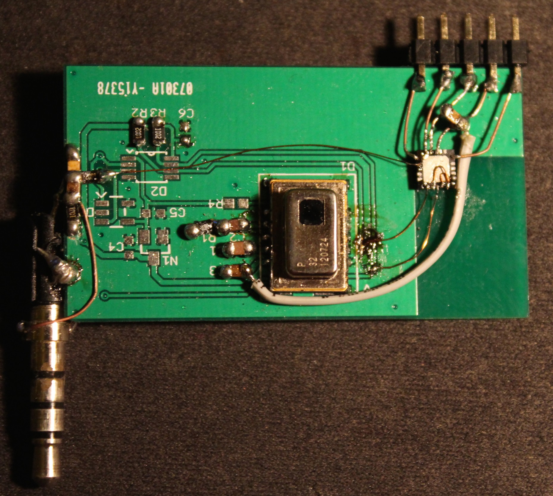
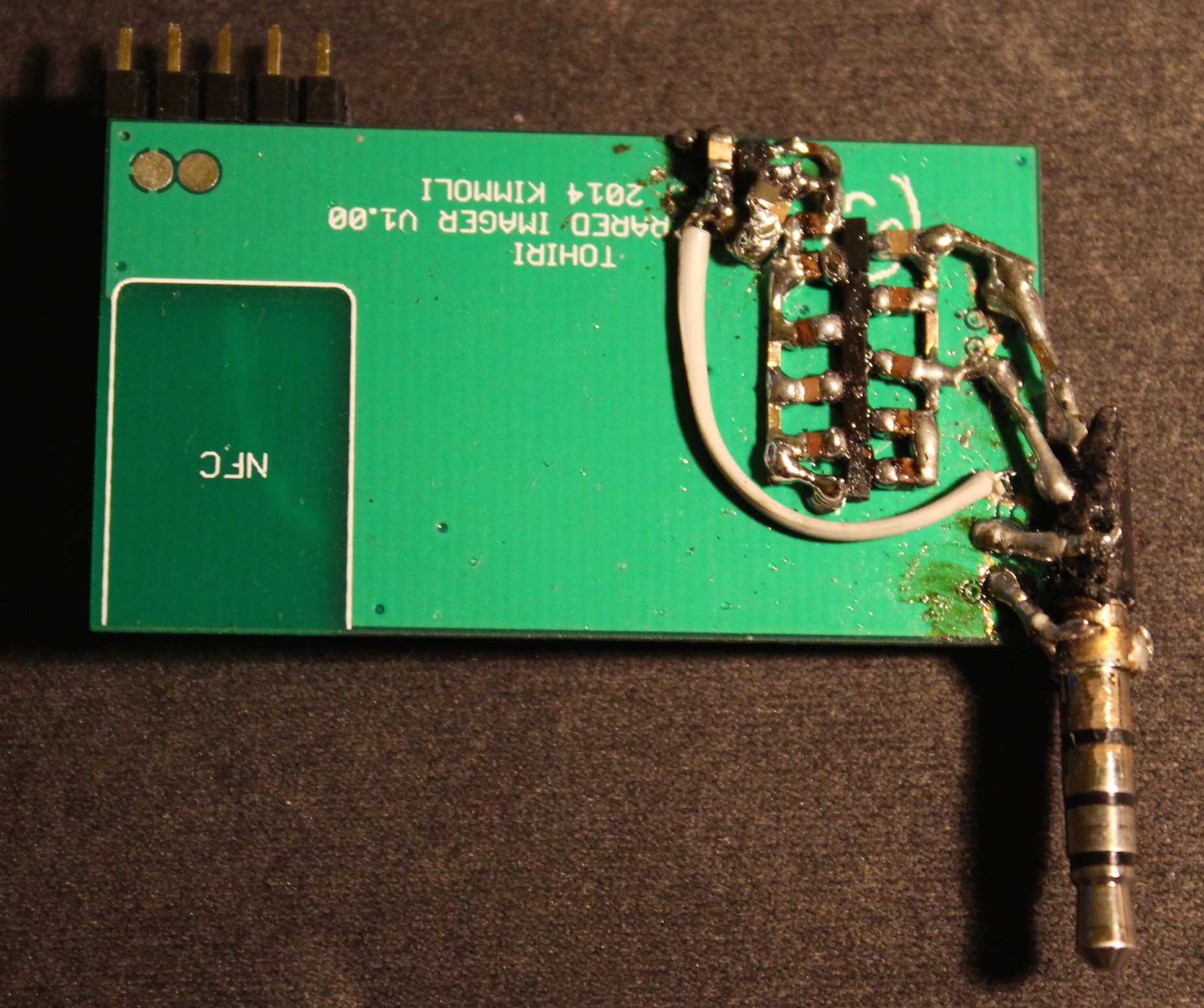
The current TJ Gen0 is a crude prototype (more of hardware hack) and consists of a Panasonic GridEye AMG8832 8x8 pixels IR FPA soldered on a modified breakout board (+components and wires hacked around it) - actually the breakout board was a TOHIRI originally, The Other Half attachment PCB for the Jolla smartphone - props to Kimmoli for providing it!)
 TJ Gen0 prototype connected to an iPad running the TJ test app
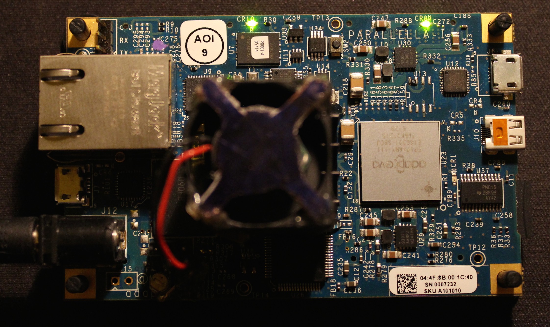
TJ is looking at this Parallella Gen1 board (see the metal plated Adapteva E16 chip in the video in darker colors and the small QFN DC-DC converter below it in hot white)
- Next TJ prototype will use an Omron D6T1616L 16x16 IR FPA engineering sample which will result in much better performance, nevertheless it's still exciting to see the performance that you can squeeze from an < $40 Panasonic GridEye AMG8832 8x8 pixels IR FPA