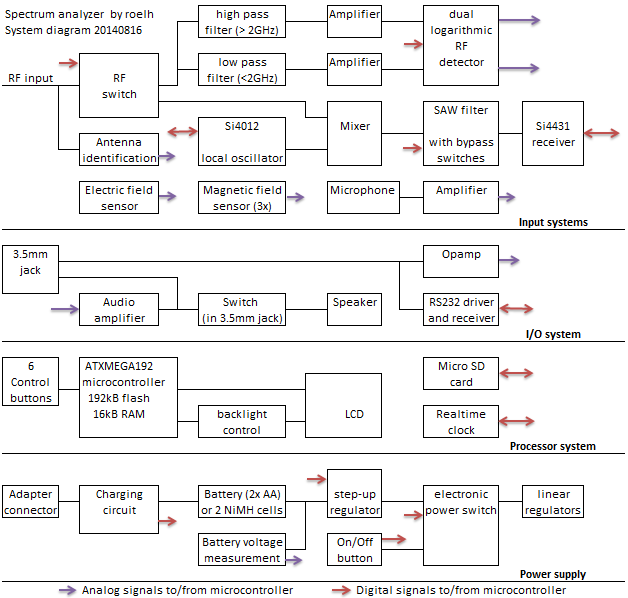
- System diagram
- Internal operation of the spectrum analyzer
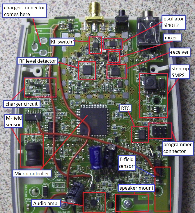
The analyzer has the classic structure with a local oscillator, mixer and IF system. The Si4012 is used as local oscillator, it generates up to 960 MHz and has a two-wire control interface. The mixer is a Maxim 2680. The Si4431 is tuned to the IF frequency (with selectable bandwidth) and provides a logarithmic signal strength indication.
The Si4431 can be tuned to 960 MHz maximum, this would give a maximum receive frequency of 960+960 = 1920 MHz. But we can also use the 3rd harmonic of the oscillator, this theoretically gives a maximum receive frequency of 3840 MHz.
For a given receive frequency, mirror frequencies are suppressed in firmware by using two or more combinations of LO and IF frequency. The wanted frequency will be present in all combinations, mirror frequencies are only present in a single combination.
The sweep time is set automatically by the firmware, as a function of the SPAN and the RBW.
- Other functions
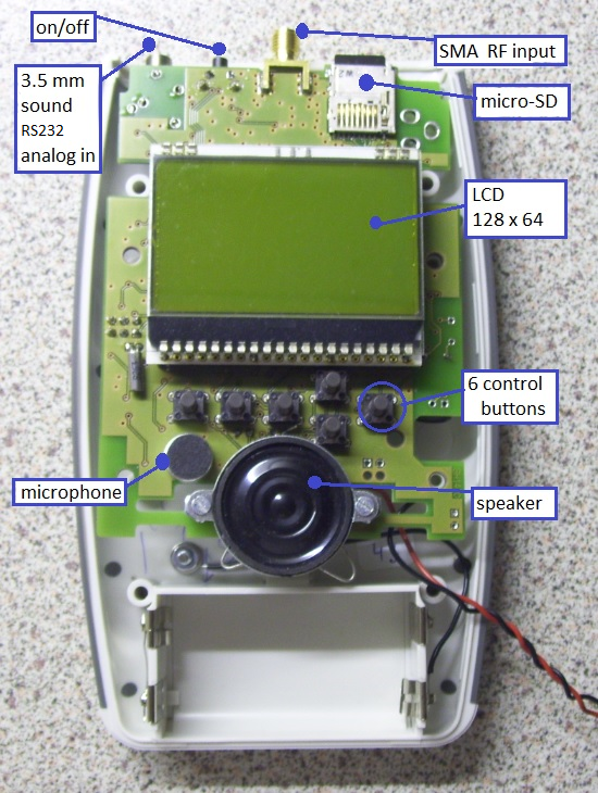
Several wireless communication systems use short pulses, that might be hard to detect on a spectrum analyzer. To detect these, the analyzer has a ADL5519 power detector that works up to 6 GHz. The power detector is sampled at 20KHz, so it will detect short pulses without the need to be tuned to a certain frequency. It also has the ability to measure the frequency of the pulses (under most circumstances with 100MHz resolution), this is described in one of the project logs. The input is switched between the spectrum analyzer and the power detector with a AS186-302 switch chip.
Every 10 seconds, the maximum output level of the power detector and the detected frequency are written to a micro-SD card. A realtime clock is present to provide date and time stamps to the logfile. The logfile is readable on the device itself, but can also be read with excel (CSV format). Every new day, a new directory is created for this day and a new logfile is created. Every month, a new directory is created for this month that contains the directories of the days.
The micro-SD card can also be used to upgrade the internal firmware.
The output of the power detector can be directed to the internal speaker, so you can hear the wireless communication pulses. The sound is generated by the DAC output of the microcontroller, with the same 20KHz sample rate. Volume control is done in the firmware. Sound can be output through a 3.5mm jack. The second channel of this 3.5mm jack can be used as analog input, or as a half duplex RS232 communication port.
A microphone is available. I want to be able to record spoken comments (and store this on the SD card) while measuring, but the firmware for this sound recorder is not yet working.
The device is powered by two AA batteries, or two NiMH cells. An adapter can be connected to charge the NiMH cells.
- low-frequency electric and magnetic fields
Many people have health problems due to exposure to RF radiation (see mast-victims.org). These people can also be sensitive to low-frequency electric and magnetic fields. For this reason, the device can also measure these low-frequency fields. The waveform is displayed on the screen, and can be output at the speaker. 20KHz sampling is used. Every 10 seconds, the measured value is written to the logfile. The same functions are available for the analog input (AC value is measured, DC value could also be measured).
- User interface
Only the most important user-interface functions are mentioned in this section.
After switching ON, you can choose between the following modes:
- SCAN (Spectrum analyzer)
- RF (Power detector)
- ELEC (electric field)
- MAGN (magnetic field)
- MENU (Utility functions: inspect SD card, set time and date)
The spectrum analyzer mode displays the following values:
- In PK (peak freq) mode: measured level and frequency of the detected peak
- In CF (center freq) mode: level and frequency at center frequency
- Start and Stop frequencies, Span, RBW (Resolution bandwidth)
- Graphic presentation of the spectrum
- Battery condition
A dotted vertical line will show the position of the displayed frequency.

The spectrum analyzer provides control in several button modes:
- SPAN :
- Step up or down through a sequence of SPAN values
- FREQ :
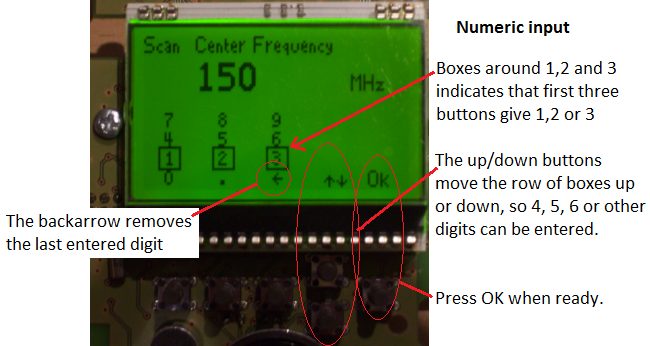
- Set center frequency or start/stop frequencies (numeric input)
- Step the center frequency up or down in half-SPAN steps
- Select CF (center freq) mode or PK (peak freq) mode
- Set CF to PK frequency
- RBW :
- Step up or down through a sequence of RBW values
- MRKR :
- Move the dotted-line marker over the screen. Level and frequency at marker frequency are shown.
- Set the marker frequency (numeric input).
- Set CF to marker frequency.
- DISP :
- Set backlight brightness
Values for center frequency or start- and stop frequency can be entered as numbers:
- Power supply design
Much attention has been given to the power supply. There is a step-up converter, built from discrete devices, that converts battery voltage to 4 volts (switchable by the ATXMEGA to 5 volts for the AG201-63 RF amplifiers for the RF power detector). To prevent interference of the regulator frequency with measurements, the frequency of the step-up converter is generated by the ATXMEGA, synchronous with (and a multiple of) the sampling frequency. At power-on, the output of the idling step-up converter is enough to start the microcontroller. The step-up converter still works at 1.9 volts input (two almost empty NiMH cells).
The output of the step-up converter powers several circuits, and also goes to a 3V3 regulator. A 0.5% accuracy type is choosen (LP2980-3.3) , because 3V3 is also the reference for the ADC of the ATXMEGA. This regulator only provides 50mA, so a second regulator is used to power other 3V3 devices.
Detailed description of the design will follow later.
- Firmware
The firmware is in C and compiled with GCC. Several sections are in assembly.
The 20KHz sample rate is made possible with the DMA transfer capabilities of the ATXMEGA. After 256 samples are captured, an interrupt occurs that processes all these samples.
The ADL5519 (and related amplifier chip) consume a lot of current. This has been reduced by switching them ON just before the ADC takes a sample, and then switch them OFF for the remaining time before the next sample. This switching is done with a PWM signal. It is synchronized to the ADC by means of the event system of the ATXMEGA192.
- Enclosure
The pcb was designed to fit a Hammond enclosure. The enclosure has a nice battery compartment. See Envionic.