 peter jansen
A very exciting post after a weekend of beginning assembly!
Motherboard Assembly
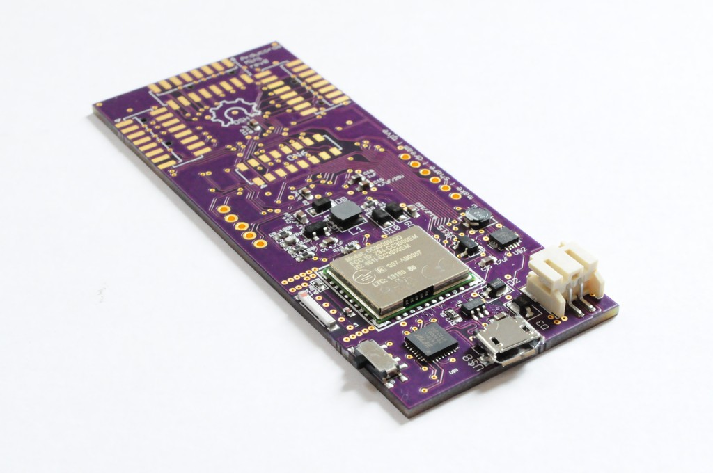
The bare motherboard PCBs and the rest of the components arrived this weekend, and I'm very happy to say that there's now a partially assembled prototype. There's of course still lots of hardware verification and software to write, but moments after finishing the motherboard I wrote a simple test for the OLED display, and took this quick test video. Of course my cat decided it was the perfect time for sits...
I remember nearly a decade ago when I first started designing and populating boards with surface mount parts, I started off like everyone else manually placing paste on each pad with a solder syringe, and then "fine tuning" these globs of paste with tweezers to make sure that there wasn't too little (which would cause a pin to fail to solder), or too much (which may cause a bridge with a neighbouring pin). Recently folks like OSHStencils have popped up, which make very inexpensive laser cut solder paste stencils. This not only saves a great deal of time, but cuts down on bridges or unsoldered pins. I'm still refining my technique -- I usually find for tight-pitch TQFPs with a bunch of pins I'll still prefer to manually solder them to reduce the chance of bridges (which can be difficult to repair), but for passives, small QFNs, or other parts with large pitches, these inexpensive solder stencils are absolutely great!
A set of tweezers and some time later, the parts on the bottom of the board are populated and ready to be reflowed.
When I first read about reflowing boards in a toaster oven, I wasn't sure what to think, but with a few inexpensive boards to practice on for your first few tries you can usually get fairly good results! For large boards sometimes you'll find the heat is a little uneven, and parts in one location of the board may reflow well before others. This certainly leads to cooking parts, especially delicate sensors, but if you watch it diligently you can usually minimize this. (Or, at least have a good idea what parts to replace when the board doesn't power correctly ;) ).
I usually try to keep all of the parts that I'd like to reflow on one side, and the parts that I'll hand solder on the other side.
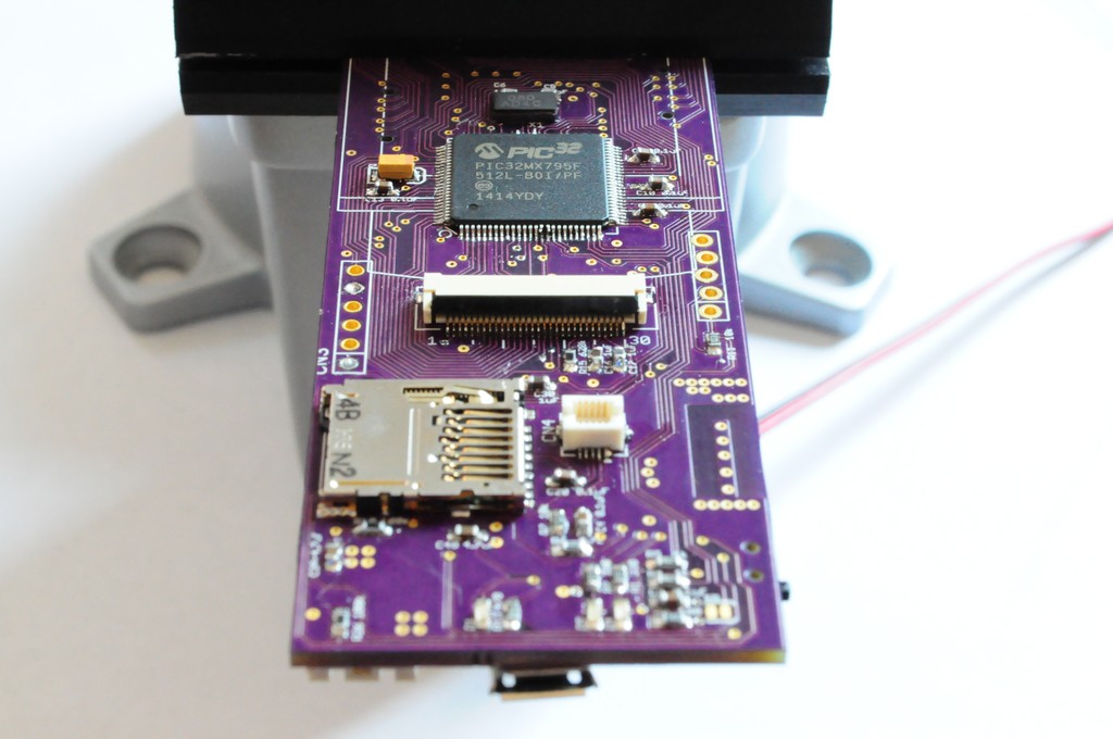
One of the Arducorder mini motherboards, after reflowing. Looks beautiful! There was only one small bridge, on the TPS63001 buck/boost regulator.
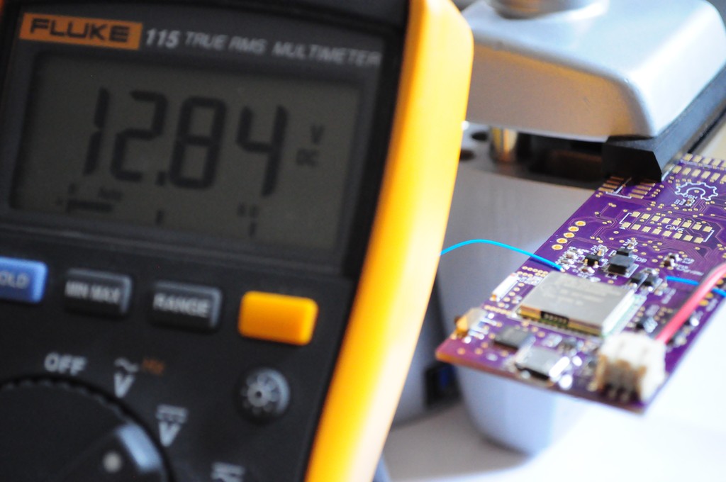
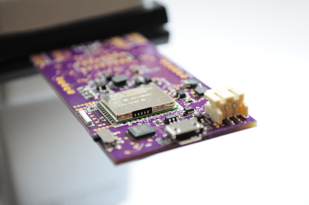
Before populating the other side of the board, if possible I like to try and test the components on the first side. For multilayer boards I tend to put the power circuitry on the bottom side, and this allows the opportunity to test the voltages before populating the other side, and help narrow down potential issues if any issues pop up.
Everyone has aspects of design that they're good at, and some aspects that need a little work. Historically I know that I've tended to over-engineer power circuits, and haven't had a perfect success rate with complex buck/boost switching regulators, so I tend to treat these as a learning experience and give them extra attention. Here the FAN5331 boost regulator looks to be working properly, and successfully generating the 13V OLED supply. Great news, and score one for following those recommended layouts in the boost datasheet!
Making your mistakes cheaply
One of the most beneficial life lessons I've ever learned is the idea of making your mistakes cheaply, which is something my mentor in graduate school used to say. I remember before going to grad school, I used to look up at all these researchers and professors and other monster minds and think -- they must be such bright and intelligent folks from all their years of experience, and rarely make mistakes. Ten years later I'm a one of those researchers, and I make ten times more mistakes than I used to -- infact, research is so challenging I sometime say that I'm a professional mistake maker, because most of what I do is try out ideas that might not pan out. The difference is that I've had ten years to learn how to make those mistakes very quickly, ideally without much cost in time or resources, and quickly move onto finding the solution.
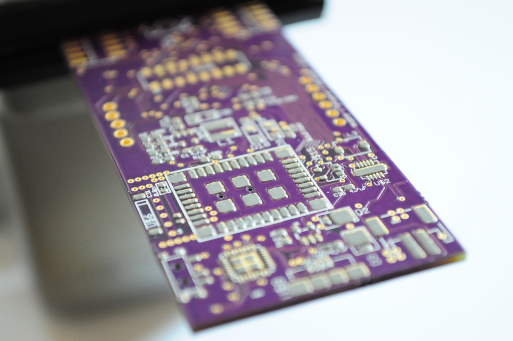
I bring this up because in the picture above (the top of the motherboard, hand populated), there is a mistake that I made cheaply this time, but only because I'd made it at a cost of days of debugging about four years ago instead of an hour this weekend. When you're in a time crunch you sometimes have to rush, and when you rush you sometimes tend to repeat your errors. Looking at the processor, can you spot the two pins on the bottom that have been lifted? Here, I've swapped the VDD and GND pins for one of the sets of power pins to the chip, causing the power and ground planes to be directly shorted. Thankfully there are many other sets of power pins on the processor that are all interconnected, so these two can be lifted until they're corrected in the next revision.
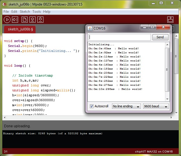
After hand populating the top of the board and resolving any soldering issues that popped up, I connected the Microchip ICD3 to the programming header, and programmed the Arduino-compatible chipKIT bootloader. It worked fantastically, and connecting to the FT232 USB-to-Serial bridge, the Arduino-compatible MPIDE successfully worked the first shot. Great news!
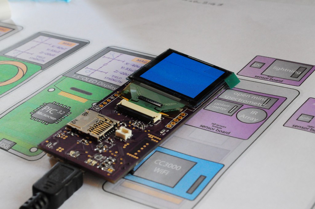
To test the OLED display, I wrote a quick driver that would access the SSD1351 display driver in 8-bit parallel mode, and fade some coloured displays in and out. This works great as well, and it was very rewarding after the assembly and verification to see a bright, beautiful organic led display light up, refresh at blazing speed, and show incredibly vivid colours. This has got me inspired and brainstorming about the user interface concept, and the best kind of test is one that gets you excited for the work that follows.
Next up is writing basic hardware and graphics drivers for the motherboard, verifying that everything works, and preparing for the touch wheel board and first batch of sensor boards that should arrive in time for the weekend. I also have to work out some measurements for the bottom (spectroscopy) sensor board, to see if I can fit in a more compact version of the spectrometer. With a large project like this on a schedule, much of the success is determined by filling the pipeline and ensuring that the next revision of boards are busy being made on the 12-day fab cycle while I'm tinkering away on the code.
Having hardware in hand is very encouraging, and things are really starting to get exciitng. Thanks for reading and to everyone who has sent in kind words of encouragement, and stay tuned!
Discussions
Become a Hackaday.io Member
Create an account to leave a comment. Already have an account? Log In.
I Like your cat ^-^
Are you sure? yes | no
Are you sure? yes | no
Otherwise the board is looking pretty nice!
Are you sure? yes | no