 PK
PKWelcome to all the new followers! The attention is appreciated (and thank you to HaD for the feature) - and it gives me hope that more folks than just us in the PK household will get some use out of this thing.
By day, I'm an engineer - and one of my responsibilities is to write a fair amount of documentation. Of course, it's usually retrospective - here's what we did, here's an application where you can use this.
Hopefully, with this project I can delve a bit more into the "why did you make these decisions?".
That way, even if I can't teach you anything, I can at least reveal my way of thinking... and give you folks ample opportunity to tell me why I'm an idiot.
Why Use an XC95144XL CPLD?
The Practical Reasons
- Cheap
- Hand Solderable (arguably - .5mm pitch is the smallest I've ever hand soldered)
- Easy to Understand
- Well supported
- 5V tolerant
The Personal Reasons
- Already have ISE Webpack on the PC (don't discount this)
- The Challenge™ *
*If you count hardware hacking as a hobby and you don't appreciate the challenge of fitting things into places they shouldn't fit (like display controllers and small CPLDs), you're in this for the wrong reason.
I mean, I've got plenty of working VGA/DVI/HDMI/RCA outputs on equipment here - there's no mandate to improve the PogoPlugs and the Galileo. This is just more interesting to me than watching TV or playing video games available to me because of some other engineer's hard work.
Okay, let's switch gears to the actual update and discuss the strategy with the next challenge - addressing the framebuffer memory. Hopefully this will be very useful to any of you folks deciding how to manage the write cycles in your video projects!
Our target is ISSI's IS61LV5128AL, an 100 MHz 4 Mbit SRAM.
Memory Read/Write Addressing & Timing
There are five approaches to addressing memory quickly in a framebuffer (that I can think of - please add more in the comments!):
- Switching Buffers - Use two memories, when one is complete, switch the read/write memories. Many modern graphics cards use this.
- Blanking - Only update the framebuffer in the horizontal and vertical blanking intervals. Microcontroller VGA/NTSC hacks like to employ this.
- Zero Bus Turnaround - This one is out due to the memory choice, but it's possible to flip instantly between reads/writes on some parts. (Part specific)
- Dual Port RAM - Let the memory handle the collisions - separate read/write ports. (Part specific)
- Interleaving Reads and Writes <- Our choice
This is an easy decision for this project. Because we don't have dual edge flip flops available on the XC95144XL, we're going to use a clock running at two times the pixel clock - so, for VGA, approximating 50.35 MHz. Because of that, we're going to have enough clock events to do this easily. No sweat, in fact - we're going to have about 5ns to spare.
We will have to commit a sin, though - by using the clock in our combinatorial logic (please forgive me!) we can make use of all four edges in the "50.35 MHz divide by 2" pixel clock. Clever or insane, you decide, but here're the critical timing constraints we need to meet (min or max, depending on what is worse):
- Read Time: 10 ns
- Output Enable OFF to High-Z: 4 ns
- Write Cycle Time: 10 ns
- Write Enable Pulse Width (when Output Enable is Off): 8ns
All Wrapped Up in a Neat Little Package
So, I told you we have 4 edges here for each fake-25.175MHz clock, each taking 19.86 ns:
Read and Write cycles require 2 edges, since 19.86/2 < 10ns. This means we need to swap read and write addresses on every rising edge.
When we turn off output enable, it actually takes 4ns before the bus is clear - so we burn an edge, meaning our read cycle is 19.86ns*(3/2).
As luck would have it, we only need to pulse Write Enable for 8ns - which means we'll meet timing requirements with almost 2ns to spare. Here's the pseudocode (where CYCLE can be 1 or 0, dividing our 50.35 MHz clock in two):
Chip_Enable: Always On

Output Enable: On when CYCLE = 0

Write Enable: On when CYCLE = 1 AND CLK = 0

Address: Read Address when OE is on, Write Address when it is off.

Data: On when Write Enable is on, otherwise High-Impedance -- Why?  Because normally the memory will be on the bus.
And here's the timing diagram, ripped out of ISim (ignore the address not changing during the first 2 CYCLEs - in the simulation, both write/read addresses start at 0s). The cursor was placed at the point when the memory will stop writing to the bus - as you can see, we have plenty of time to spare:
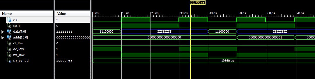
Also note: active low signals.
Closing Thoughts
I'm actually a bit behind on updates - please forgive me, videos are kind of hard to make. The PCBs have been ordered for my version 1 reference design, so I will be adding schematics, gerbers, and KiCad collateral to the Github repo soon (maybe Saturday during the day?): https://github.com/dqydj/VGAtonic
And, yes, I'll be talking about where the PCB was... how do you say... a bit 'suboptimal'. But it'll work - fingers crossed!
Discussions
Become a Hackaday.io Member
Create an account to leave a comment. Already have an account? Log In.