John Boyd
Theory:
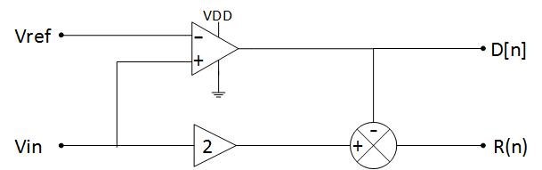
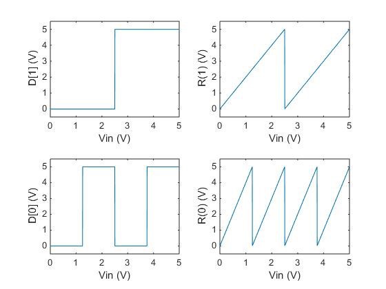
The residue amplifier pipeline ADC consists of one key block: the residue amplifier. These residue amplifier blocks are then connected in series, forming a pipeline, hence the name. The figure below shows a residue amplifier. As you can see, it takes an analog input and a "threshold" input, and then has a digital output D[n] and an analog residue output R(n) that represents the "remainder" of the input voltage - the 1st bit voltage or Vin - Vref.
Residue amplifier block diagram:
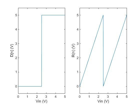
Residue amplifier output vs input plots:
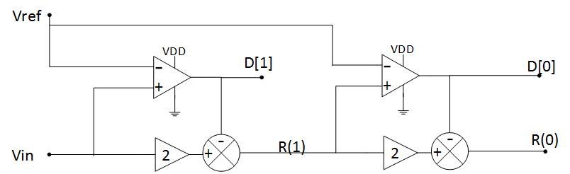
If we cascade multiples of these together, passing "R(n)" output of one stage into "Vin" of the next stage, we will have an ADC with each stage's "D[n]" representing the ADC data bits. Notice that D[0] and D[1] in the plots below represent the digital level of the analog input voltage!
Two bit ADC block diagram:
Two bit ADC output voltage vs input voltage plots:
Now how to build it:
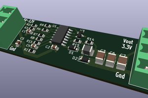
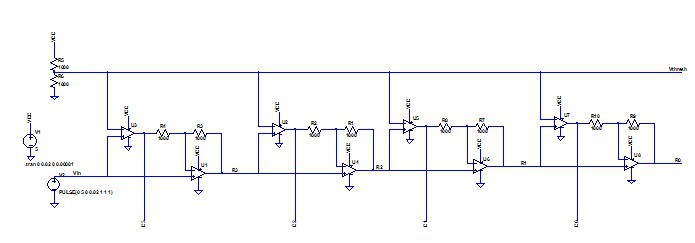
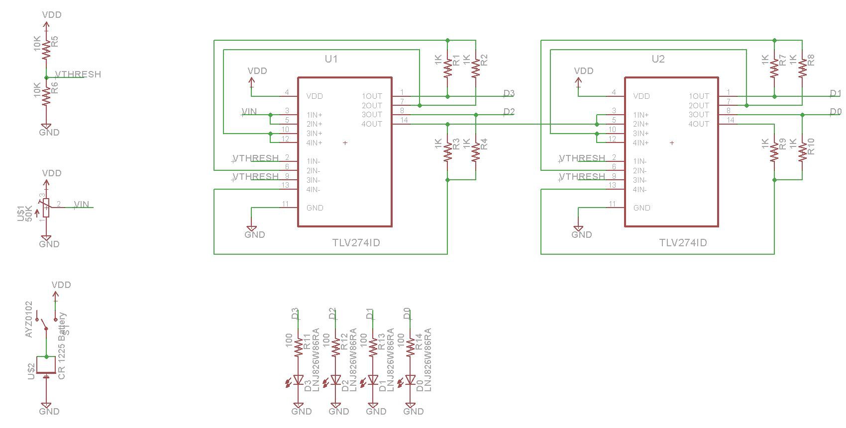
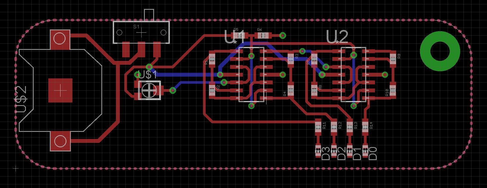
To design this kind of ADC, I just used some opamp logic to make a residue amplifier and then cascaded four of them together to make a 4 bit ADC. Below are the schematics for my design. I then just drew up these schematics in eaglecad, laid out a key-chain shaped PCB and ordered them from OSHPark.
Residue amplifier schematic:

4 bit ADC schematic:
EagleCAD schematic:
EagleCAD layout:
 matseng
 Evangelos Petrongonas
 agp.cooper