 Christoph
General thoughts
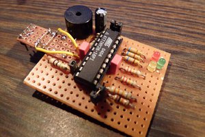
Commonly used to switch Nixie Tubes is the K155ID1 (74141). Nice: it's also a BCD to decimal converter. Not Nice: You can only get old stock which has been lying around for decades. And since Nixies are getting more popular prices increase. So let's build our own.
Problem are the voltages. Nixie Tubes have an anode voltage of around 100-200V. Tricky question: What's the cathode voltage when switched off? I'm serious, what is the answer? Since there is no physical connection between cathode and anode it's something in between depending on the switching state. If you're not sure expect the worst case, so I wanted a way to safely switch 200-300V even so I assume the real Voltage drop is much lower.
That's why I will use the MPSA 42 NPN High Voltage Transistor which has a maximum Collector-Emitter Voltage of 300V. You might simply connect on transistor to one digital IO of your favorite microcontroller. But that scales badly. One Nixie (Digits 0-9 and Dot): 11 I/Os, two Nixies: 22 I/Os, and so on.
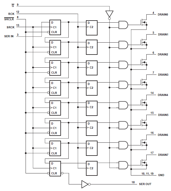
Lets use a shift register. Google for TPIC6B595 if you want to check out the datasheet. Any other shift register will be fine too, I used what I had available. Let's recall how a shift register works.
Note that tis very special one has FETs at it's output to driver higher loads. You have a single one-bit serial data input (SERI IN) feeding the first One-Bit-Storage (D-FlipFlop). The Output of the FlipFlop feeds the next input and so on. Typically you have a set of eight Bit-Storages since we live in a binary world. The last Bit-Storage outputs it's value as "SER OUT" for cascading multiple shift-registers (or other uses). Applying a clock (SRCK) makes every bit-storage "save" the current input state (high/low) and deliver it to the output. By cascading the Bit storages in a serial way we created a shift register. Since the output word (8 bit) of the serial cascaded array (may) change/s at every clock you want to have control about when to deliver the output to the driving side (right hand FETs). That's why there are an additional 8 D-FlipFlops which you clock (RCK) after your serial data is completely clocked into the input side. Everything else is just convenience. SRCLR\ lets you asynchronously (timing unrelated to SRCK) clear the input stage (set all to 0 or low). You can also clock in 8 zeros. G\ disables the output stage of driving the FETs. For basic applications you need SER IN, SRCK, RCK. Apply a constant 0 (ground) to G\ and SRCLR\ when not in use.
That's a maximum of 5 IO/s vs. 11 per Tube. Half way there!
Looking at Datasheet
Datasheets are not always easy to read, especially when you're not too familiar with the technical background. Check the maximum ratings. Supply voltage (max. 7V) and logic input voltage (-0.3 to 7V). What controller are you using? What's the IO output and supply voltage? Crosscheck the recommended values. Supply voltage Vcc: 4.5-5.5V. When using a more modern controller running with 3.3V is there 5V available at all? Check the Voltage levels for High level input 0.85*Vcc (4.25V@5V) and low level input 0.15*Vcc (0.75V@5V). Check timings. Setup time, Hold time, Pulse duration (20,20,40ns).
Do you meet all criteria? I am using an ARM Cortex Board running on 3,3V. 5V is available from USB port. The 3.3V IO output voltage is below the recommended 4.25V. Truth is, it works with 3.3V as well but that's out of specs. So don't do for device that you depend on. In that case use a level shifter. What about the timings? How long does it take to switch an IO? How do you check that? Think of your clock frequency of your microcontroller. In my case (Stellaris Launchpad) it is 80MHz the fastest possible switching time would be a single instruction (1/80MHz = 12.5ns). Well that is a close one on this uC. Since I am using some libraries to set the IOs there's additional timing overhead coming from calling and returning functions etc. If the code is extremely optimized you may run into problems and if you're running...
Read more »

 Klaus Dormann
I've read with interest your post on driving the cathodes in various ways. I have a clock design using 6 TPIC6B595's to drive cathodes directly (four ZM1040 tubes) which has been working for several years. I don't see why the added external Zener is required. The data sheet states (and shows in the output schematic) that the output is clamped with a 50V Zener between the drain and gate. When the output is off, as the voltage on the drain rises above 50V the Zener will begin to conduct and start to turn on the FET. As the FET starts to conduct, the voltage on the drain will drop in proportion to the current flowing through the FET. An equilibrium is reached where there is where the Vds is held at around 50V (depending slightly on Vth of the FET).
The only questions in terms of operating the outputs this way is if the 50V is sufficient for proper cathode selection and if the allowed dissipation and junction temperature of remain within the IC's specs. 50V is right at the low end of the recommended cathode selection voltage for most tubes. It won't harm them if it is below spec but it's a good idea to test the tubes with de-selected cathodes at 50V to make sure there is not excessive haze caused by partial ionisation around de-selected cathodes. I have found larger tubes are fine but smaller tubes can be borderline. In terms of dissipation, the worst case cathode leakage current (for the tubes with sufficient data available to calculate it) at 50V it is well under 100uA in every example I have seen so a safe calculation for the worst case dissipation is (50V x 100uA) or 5mW per channel or 40mW over the entire package. The junction temperature will remain well below the maximum right up to the maximum case temperature.
If the selection voltage is a little low for the particular tubes used then the HV5812 might be a better choice and still keep the parts count down.