 Benchoff
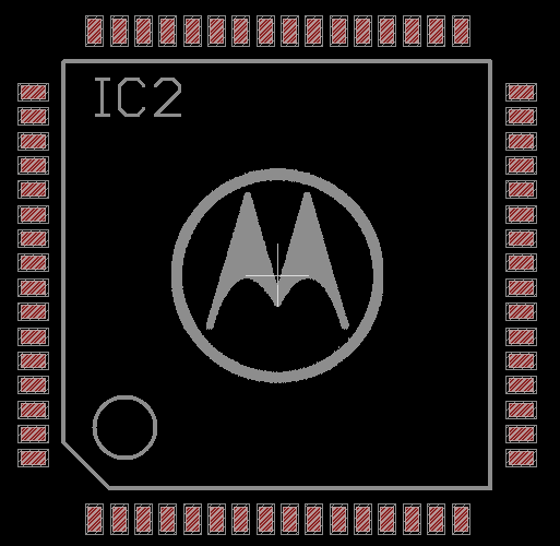
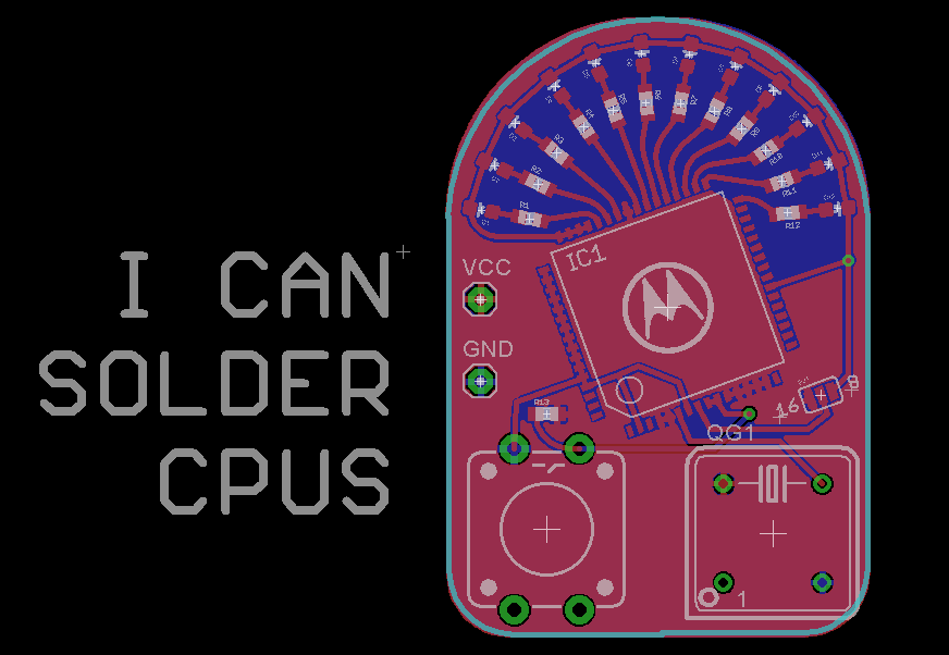
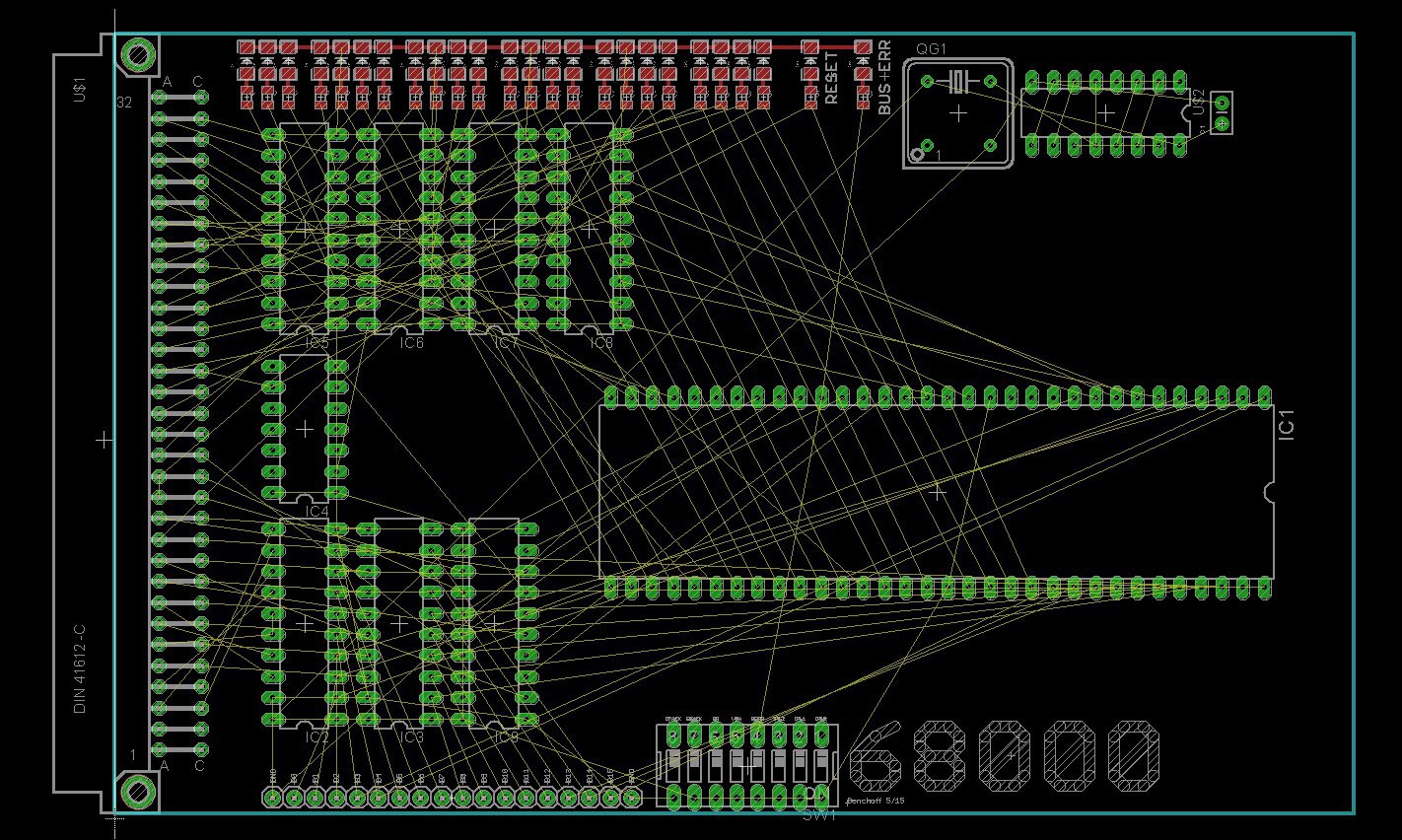
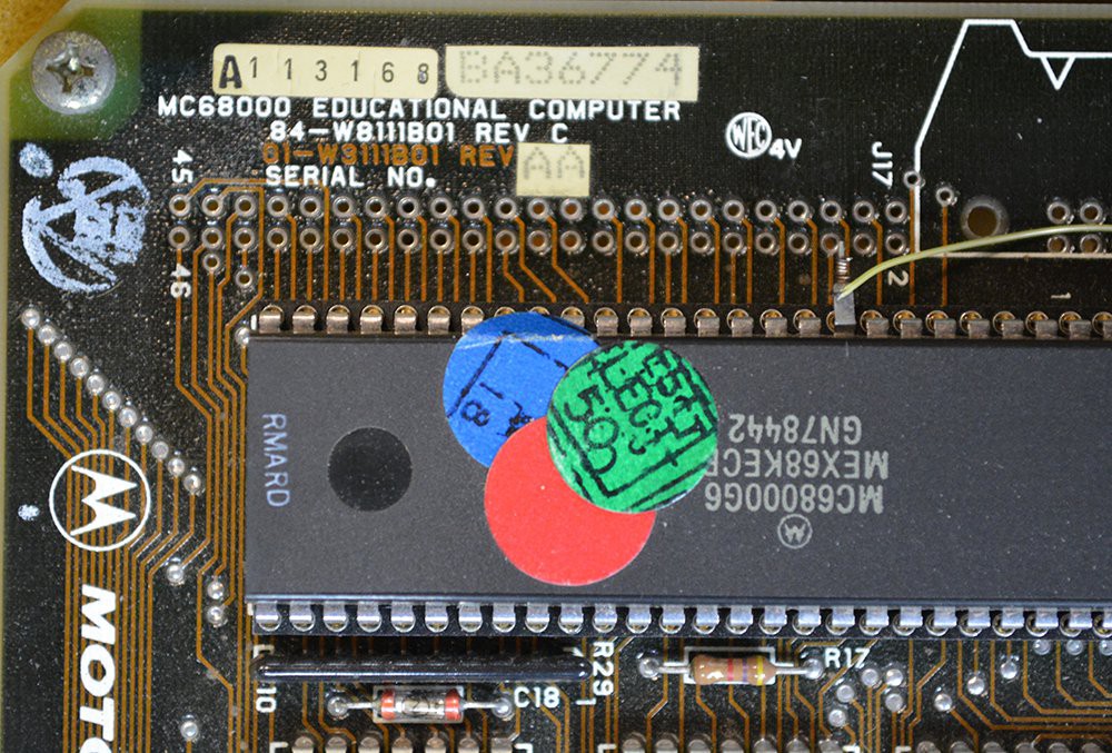
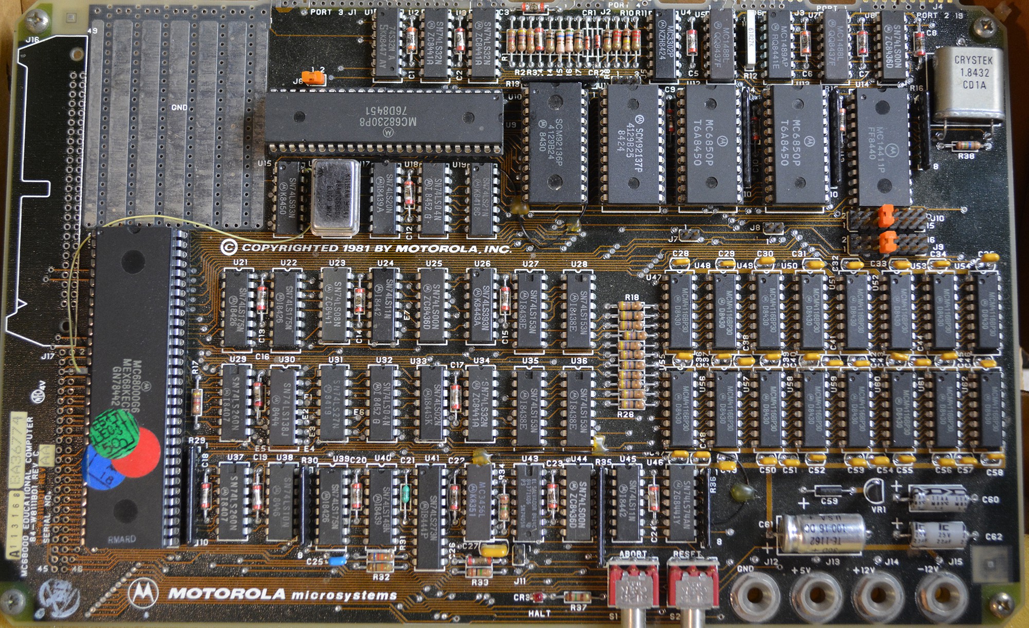
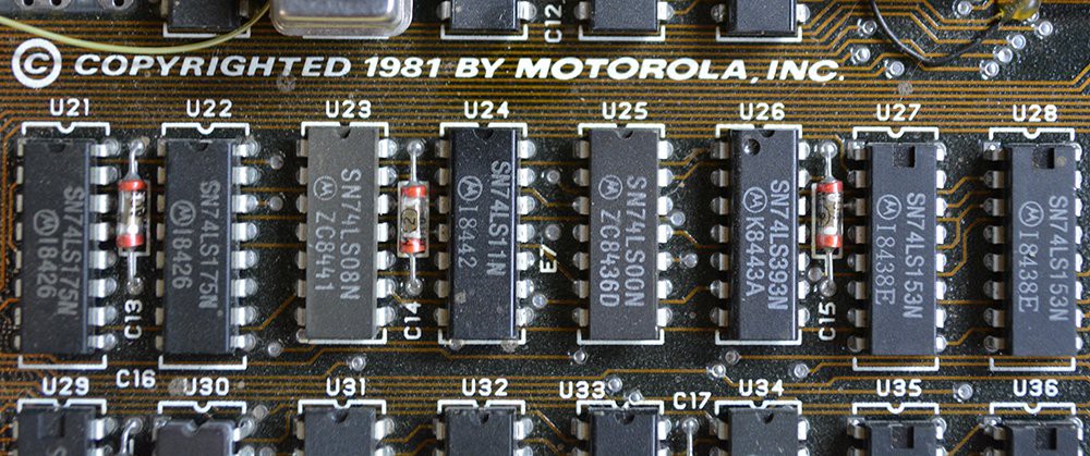
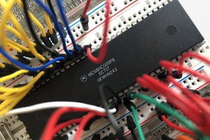
This project is a homebrew computer based on the Motorola 68000 CPU. Design includes four megabytes of RAM, 128kB of ROM, Something for video, two serial ports at 9600 baud, and eventually networking and a hard disk.
The purpose of this computer is two-fold: To show it's really not much harder to build a 16-bit homebrew computer than it is to build an 8-bit homebrew computer, and to build a server for Hackaday's retro site.
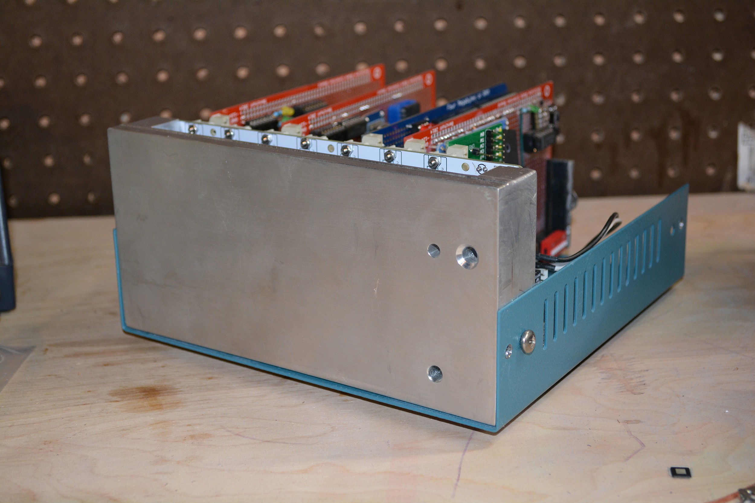 That panel was made by the SeeMeCNC guys when I was up there for the Midwest RepRap Festival. I traded a gigantic (5 foot x 8 foot) hackaday flag - made by me - for the CNC work. All the relevant files are up in the Git.
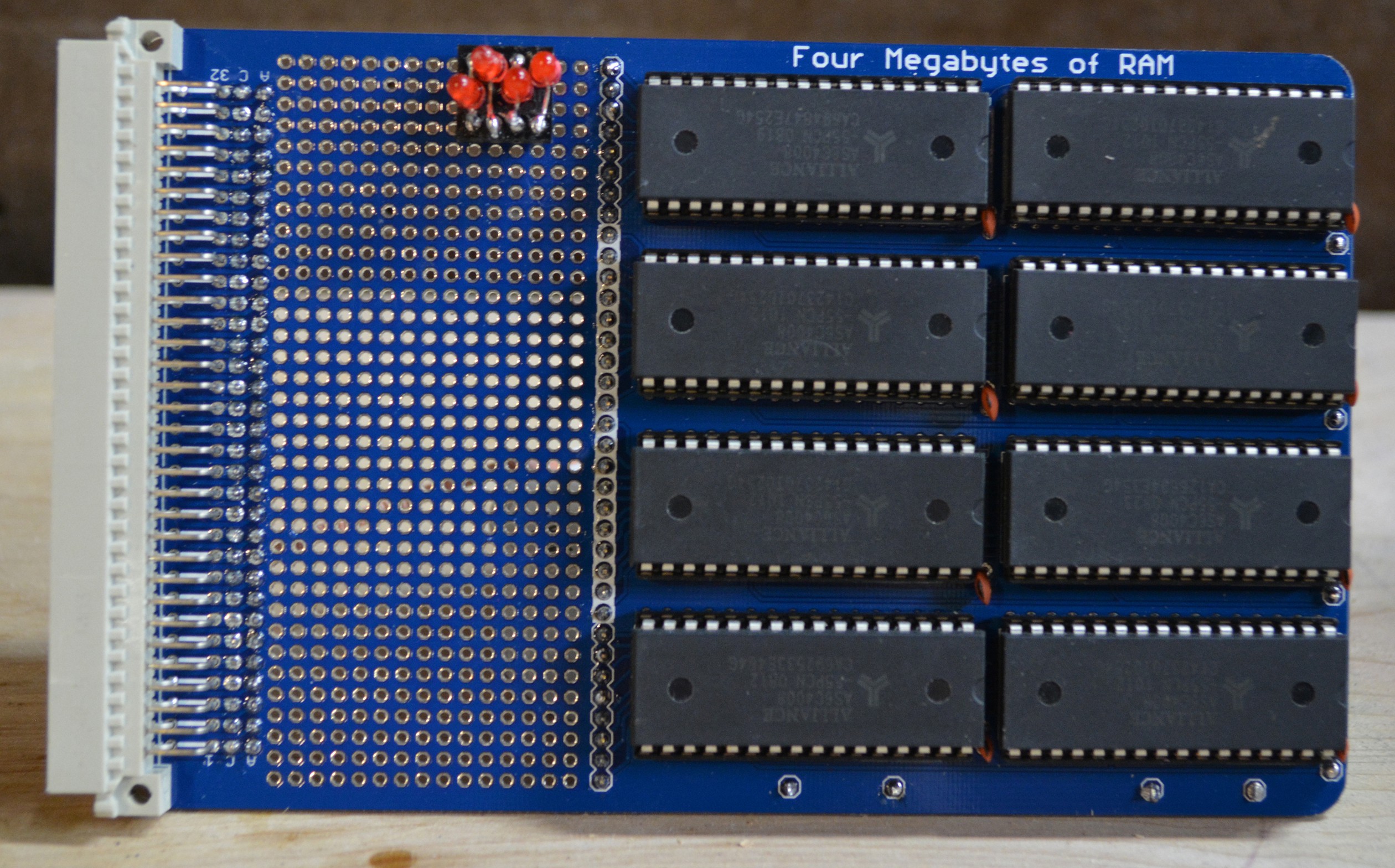 I hated the wirewrapping on my RAM card. The initial plan for all of these cards was to prototype them with wire wrap, then build a board. I met myself halfway on this one.
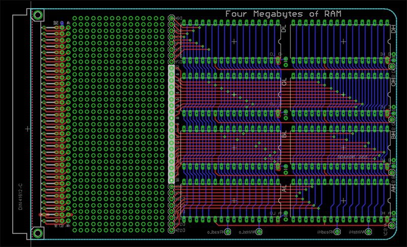
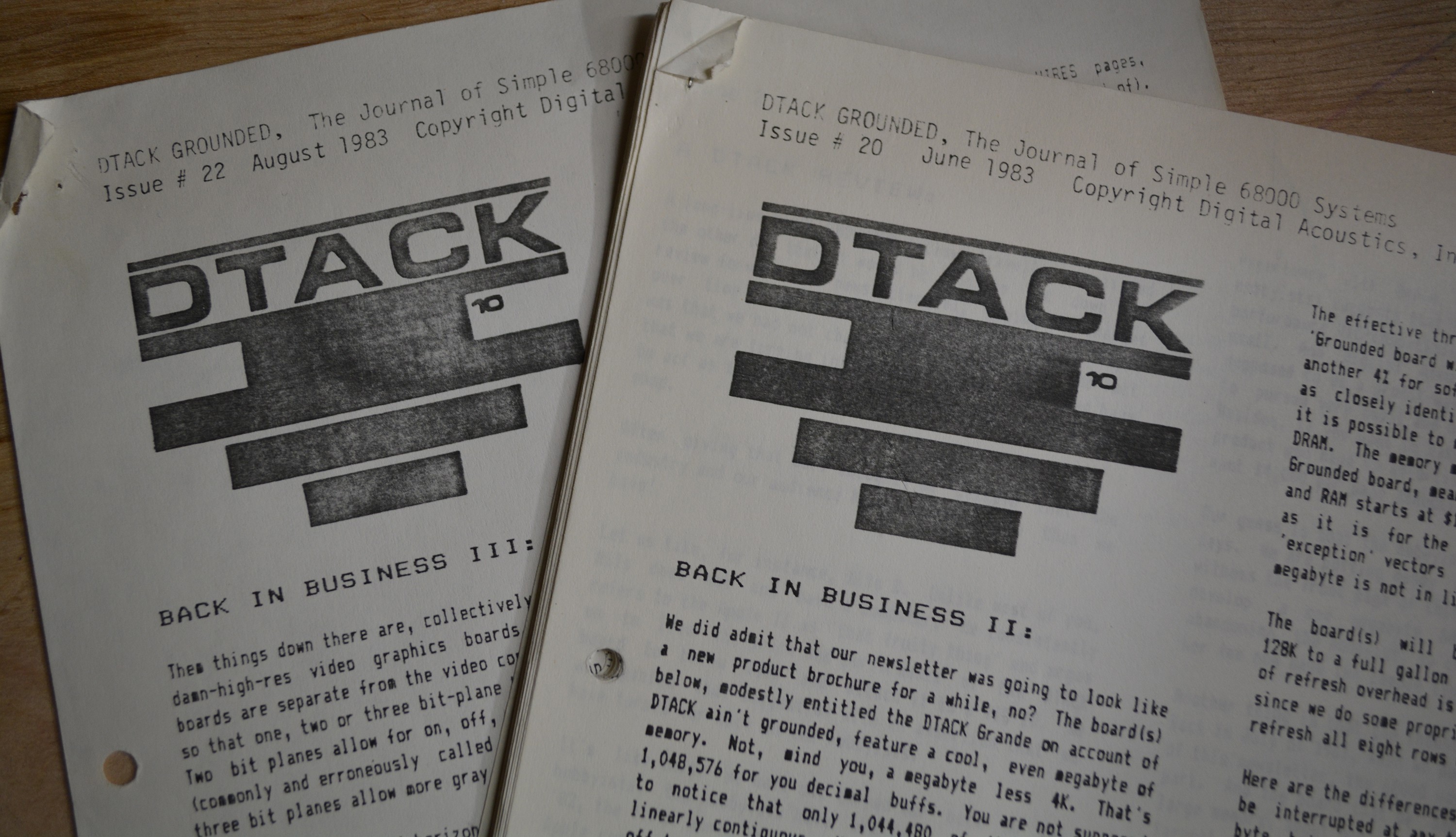 I have most of DTACK Grounded.


 Roman Romanchuk
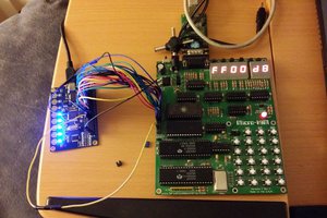
 Jac Goudsmit
 Jason Westervelt
I see you've got a comparable assignment, possibly we are able to share thoughts! I became also considering the use of a battery and static RAM chips - but the equal barriers nevertheless observe I suppose. Maybe I need to layout a SPI controller for the Z80 bus for interface with spi memory chips. read more here https://watchfulgeek.com/