 zaphod
disclaimer:
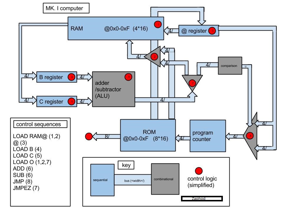
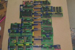
a lot of what is below is wrong. the project has gone through some major design changes, including: new architectural setup, new command set, new mechanical layout. this is the new architectural set up:

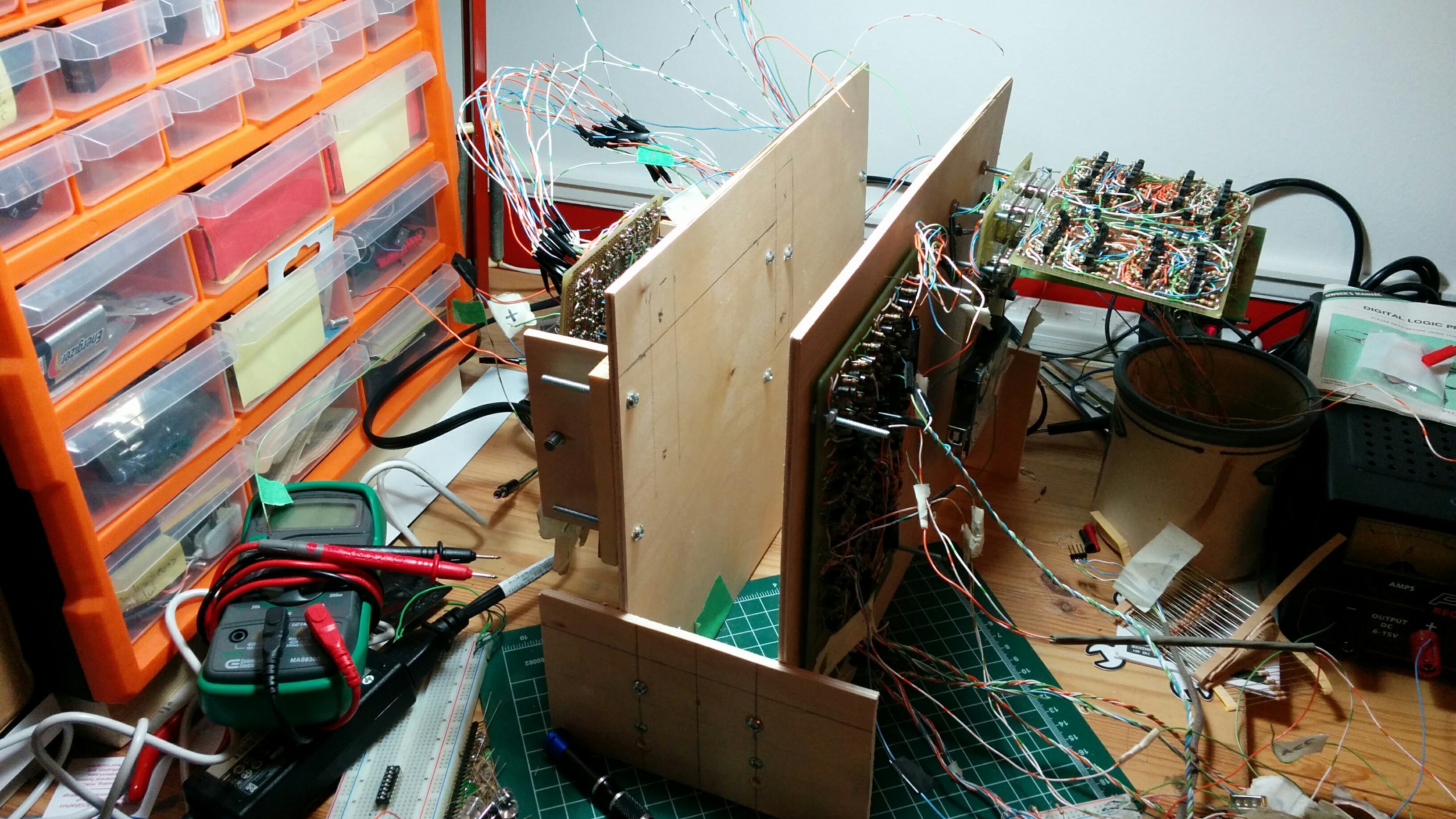
this is the new mechanical set up:
you can read about the architectural changes here.
and you can read about the command set changes in an up comping post.
I will change the below information at some point in the future.
I'm a beginner and know very little about how computers work, this is an educational project. If you find mistakes or have relevant information concerning computers feel free to comment.
The computer follows 'Harvard architecture' (I might be wrong) it has a strictly separated RAM and ROM. 4 bit is a loose indicator of bus width, the ALU is 4 bit and all the processing logic is 4 bit as is the RAM, however the ROM width ('word' length?) is 8 bits as some of the instructions contain a 4 bit value embedded.
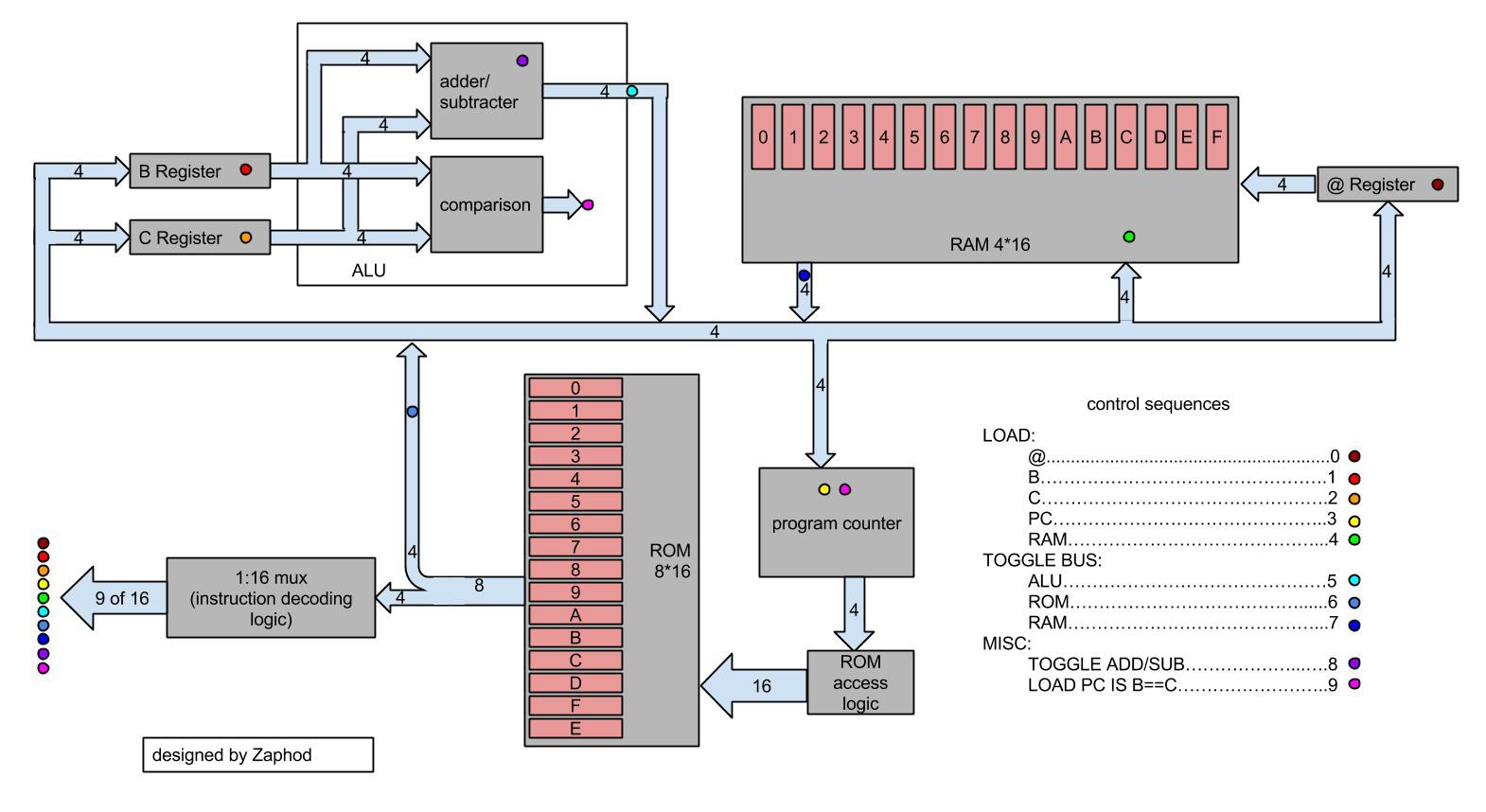
here is the architecture diagram for the computer:

major blocks:
RAM:
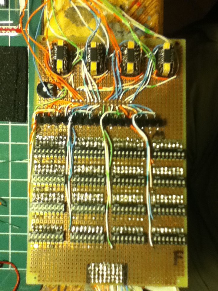
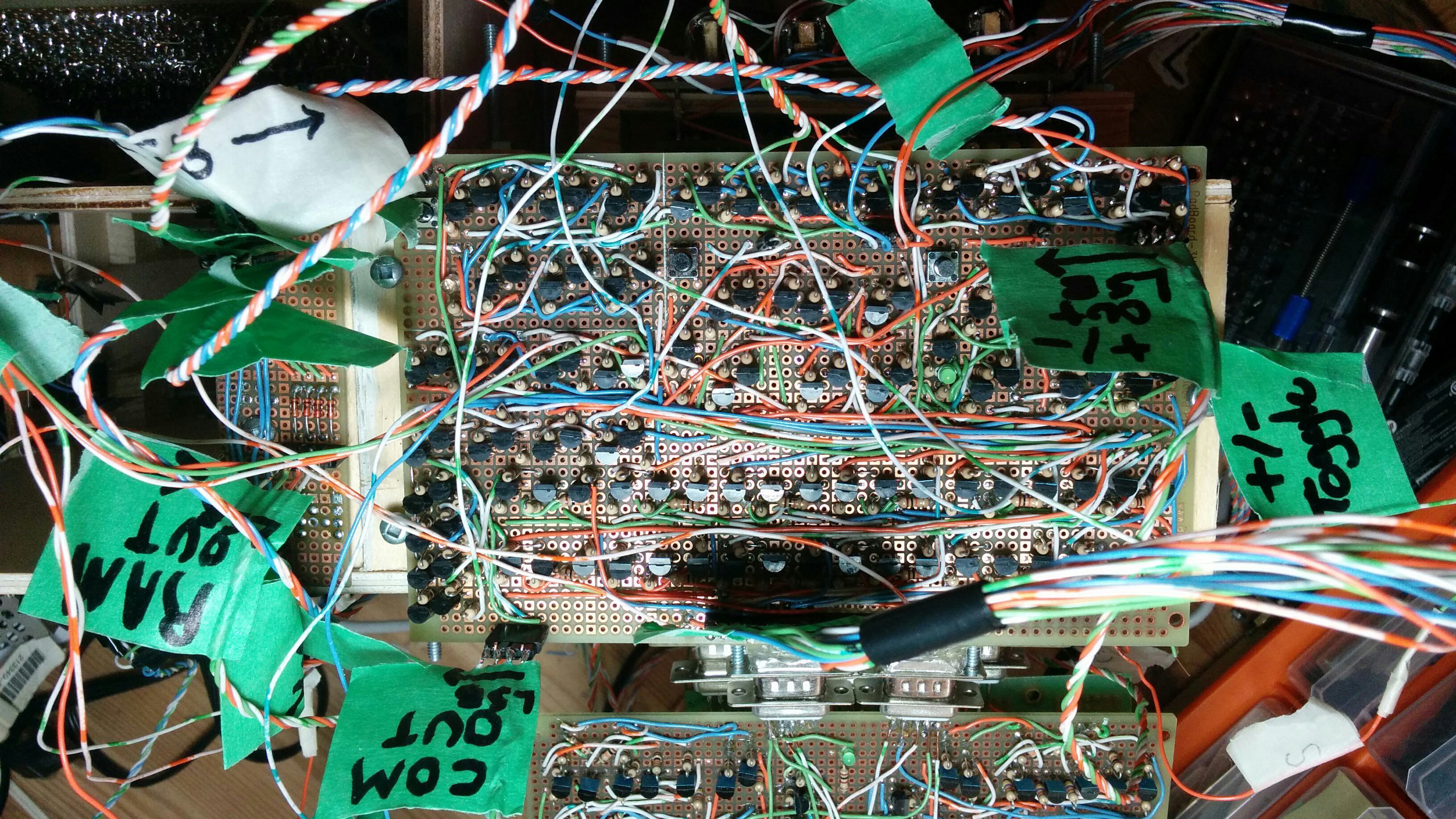
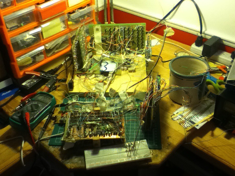
You might have noticed the Arduino in the (inexplicably upside down) photo. the Arduino is serving as memory, originally I had wanted the Arduino to only simulate a block of D flip flops but there are nowhere near enough pins on any microcontroller (that I know how to use) to do that, as such the Arduino also simulates some of the memory access logic. The Arduino will also serve as the only source of output, it basically just streams the contents of an array to my laptop through the serial monitor in the Arduino IDE, nothing fancy, I know, but it works. And before anyone tells me not to embed an entire Arduino board, this is by no means a finished project, I just wanted a simple way to to avoid soldering 640 transistors.
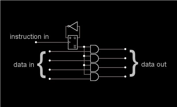
ROM:
The ROM access logic consists of a 1:16 demultiplexer with the input held high (which has been a source of quite a few problems). the memory consists of 16 dip switches and 128 diodes.
ALU:
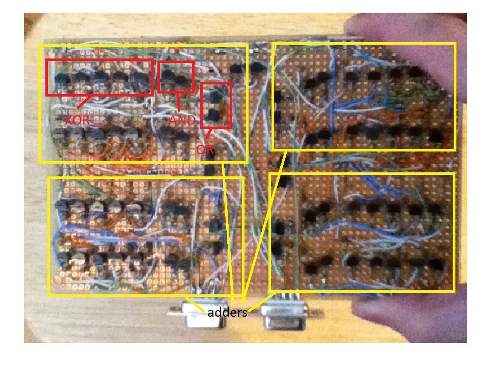
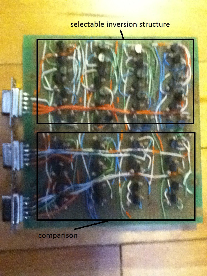
The ALU is actually just a 4 bit ripple-carry adder/subtracter. The above picture shows the 4 bit adder. To preform subtraction it uses 2s compliment math. The logic necessary to perform the invert consists of some multiplexers and inverters. The add one is done by using the extra bit on the first full adder in the adding circuitry. There is also a 'comparison unit' which will eventually be responsible for actuating the JMP (jump) command, but strictly speaking this is not part of the ALU.
each line of transistors operates on one bit, hence four lines.
Registers:
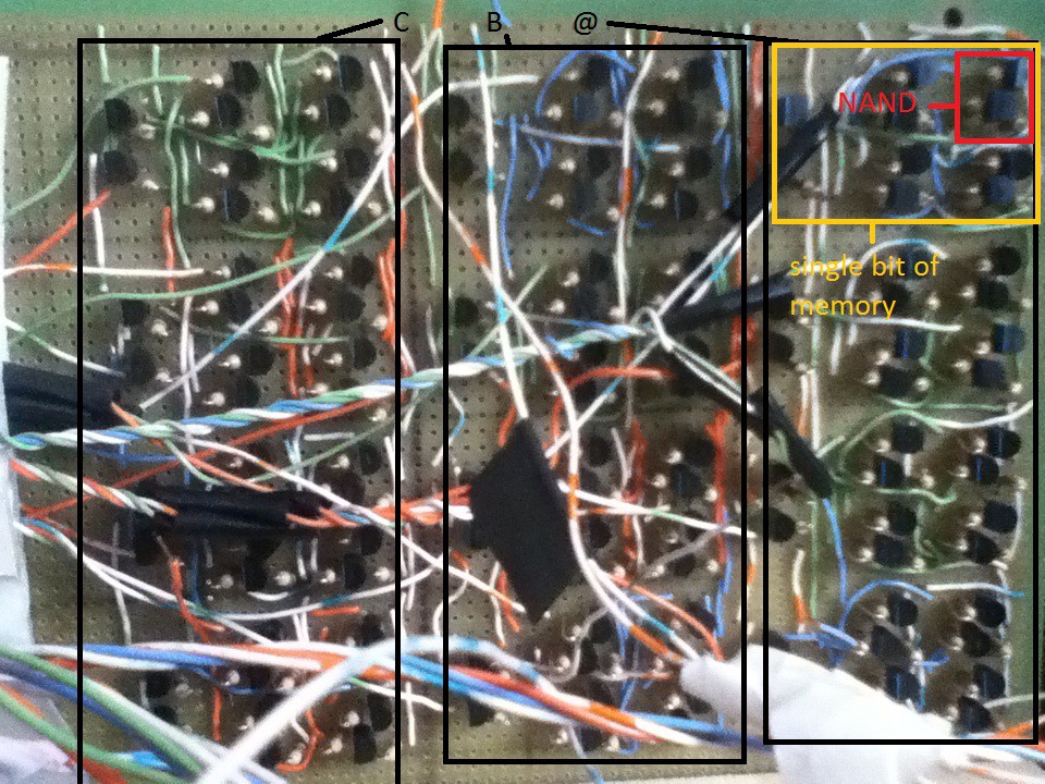
there are three registers. the first is the @ (address) register, it points to a location in the RAM with the current value to operate on. The second and third are the B and C registers, these registers are tied to the inputs of the ALU they contain the value for the ALU to operate on. While the registers could be considered memory I have decided to build these by hand. They consist of D latches built from NAND gates. Each latch requires four NAND gates, there are 12 latches total.
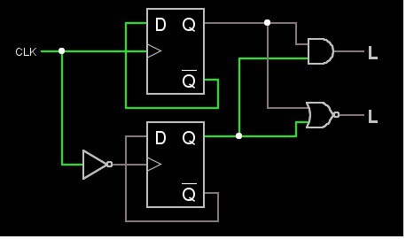
program counter:
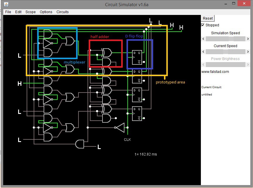
The above image was made with circuit simulator.
the above image is of the program counter in it's current state.
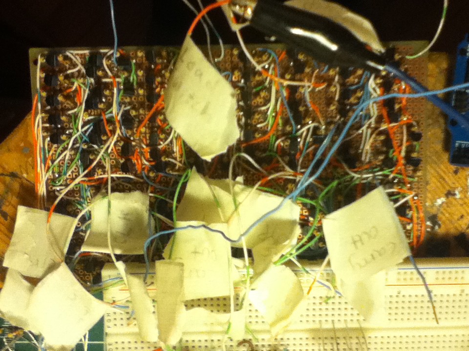
program counter construction details were posted in the project logs section.
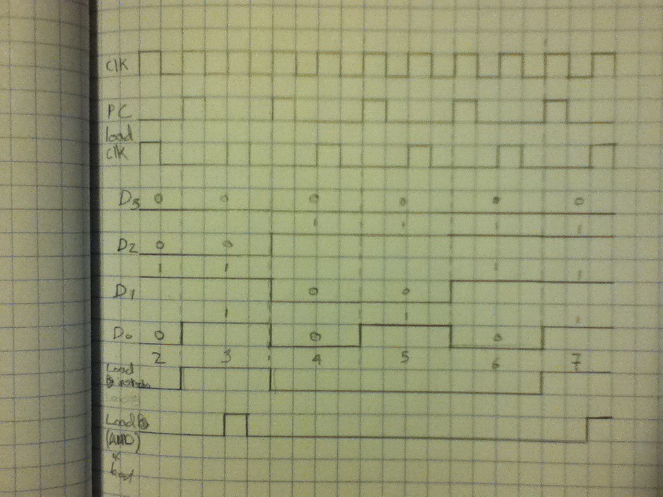
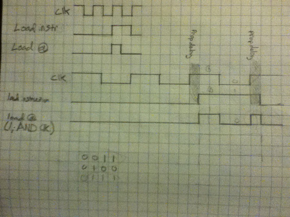
The program counter's job is to count up by one in binary every clock cycle, and output the result. the output of the program counter then points to ROM address that contains the next instruction to execute. In addition to counting the program counter also has to be re-loadable by the program, I.E. the program should be able to dictate the memory location of the next instruction. Since the program can reset the program counter loops can be implemented. In addition to this if the re-loading of the program counter if done conditionally 'if' statements can be implemented.
The program counter consists of multiplexers, half adders, and D flip-flops.
these are the major blocks of the computer, there are a lot of areas I have glossed over, (control logic anyone?) but this should give you a rough idea of what...
Read more »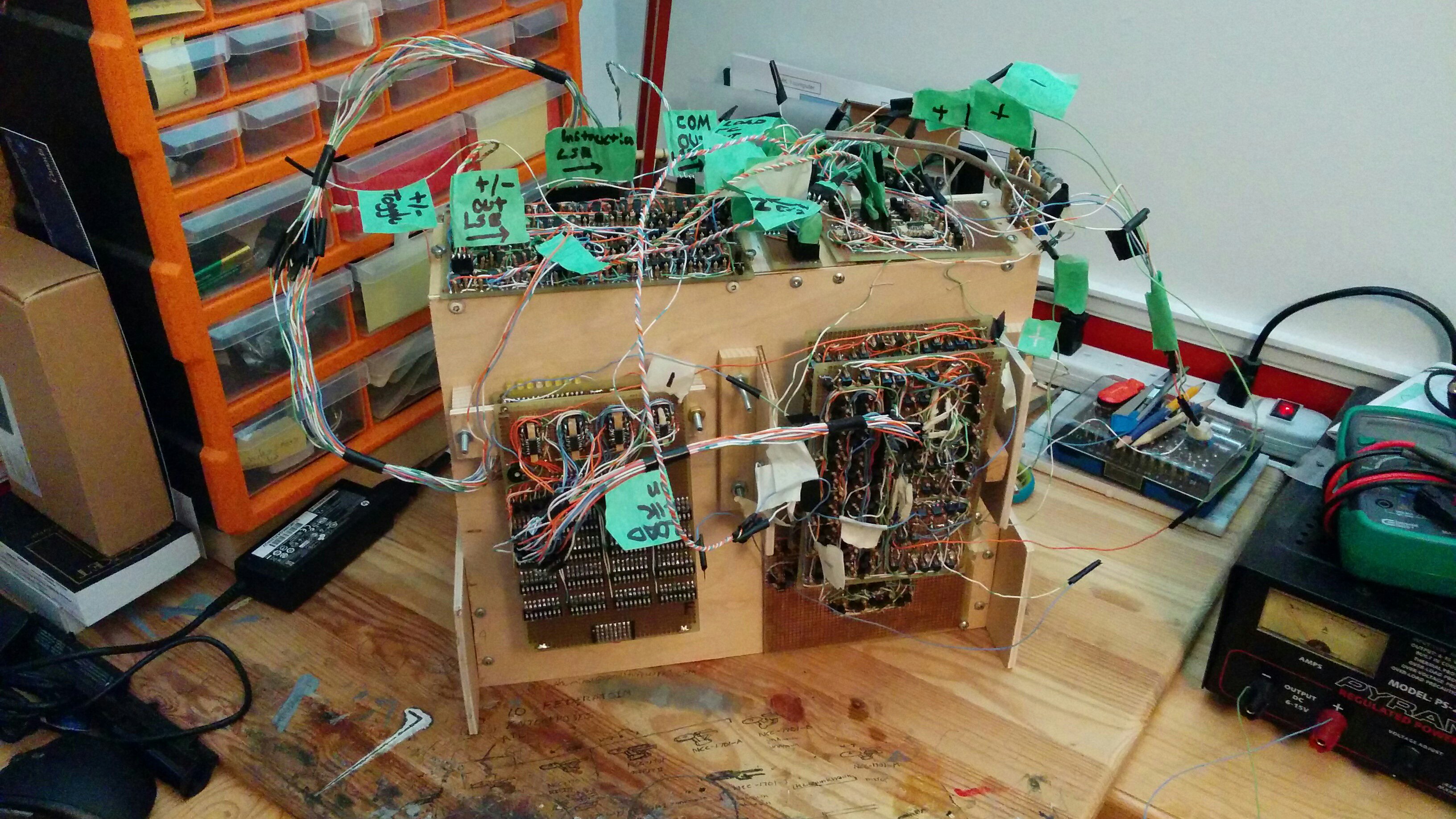


 Charlie Smith
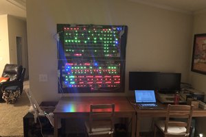
 spudfishScott
 Brandon Reinhart
 agp.cooper
Amazing work, that is really impressive!