 Dylan Brophy
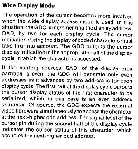
 As it turns out, I don't think I can get it to add 4 instead of just adding two as described above; this limits my maximum clock speed to 24Mhz (32Mhz on the faster Z7220), so the maximum resolution would be limited by this. On the other hand, the uPD7220 supports interlacing, so I might be able to push out a higher resolution that way. Without interlacing under this config, I can't even get to 640x480, but with interlacing I can get at least to 720x480. I'll have to play with the settings.
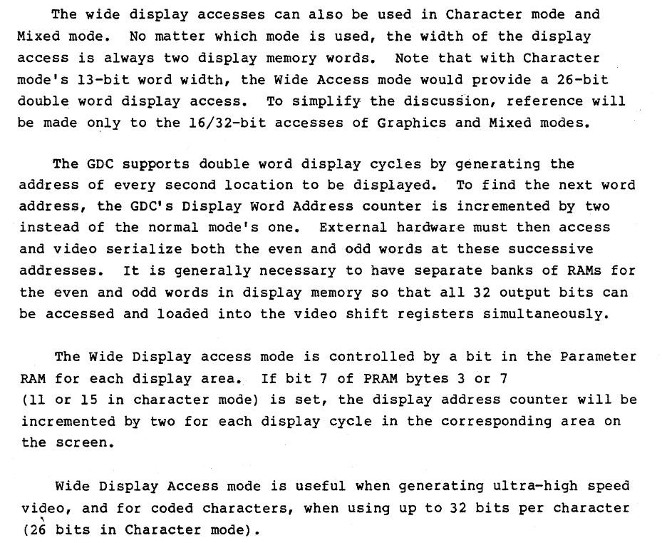
I'll need to add a 16-bit register to handle this, since I don't have a real 32-bit bus to load color data from:
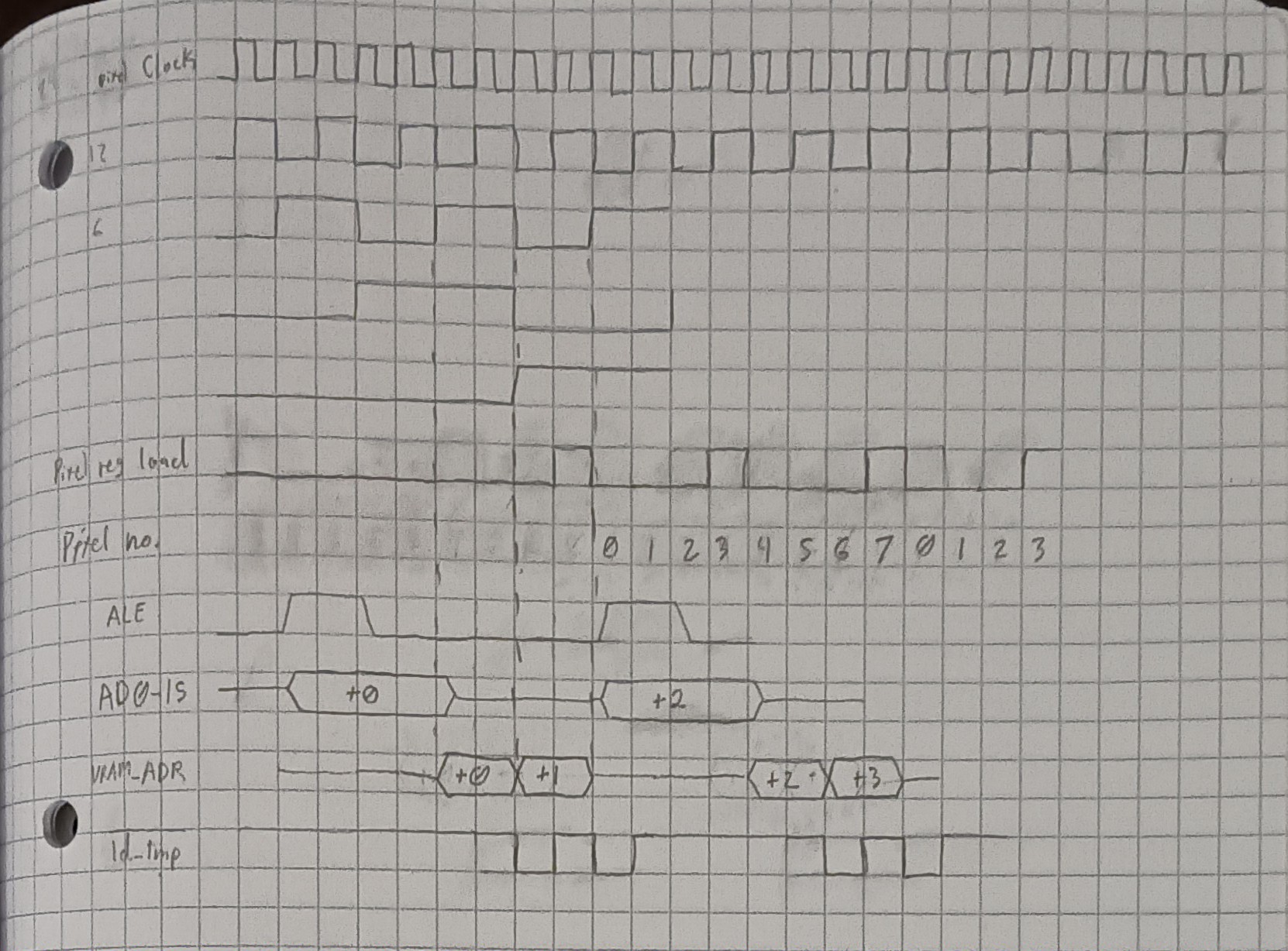
The waveforms should look something like this:
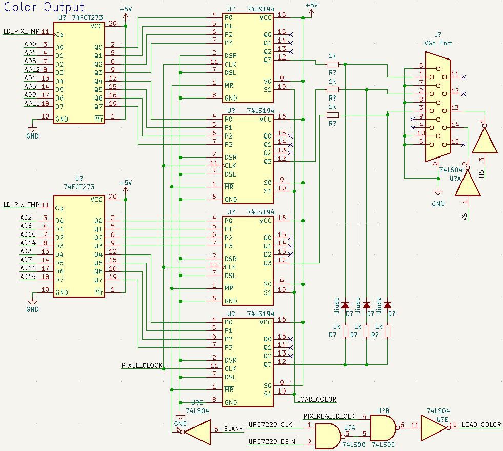
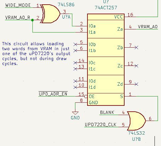
Here's the logic I designed to generate this waveform:
 As a bonus, I'm including a timing diagram from the datasheet so it is easier to find later:
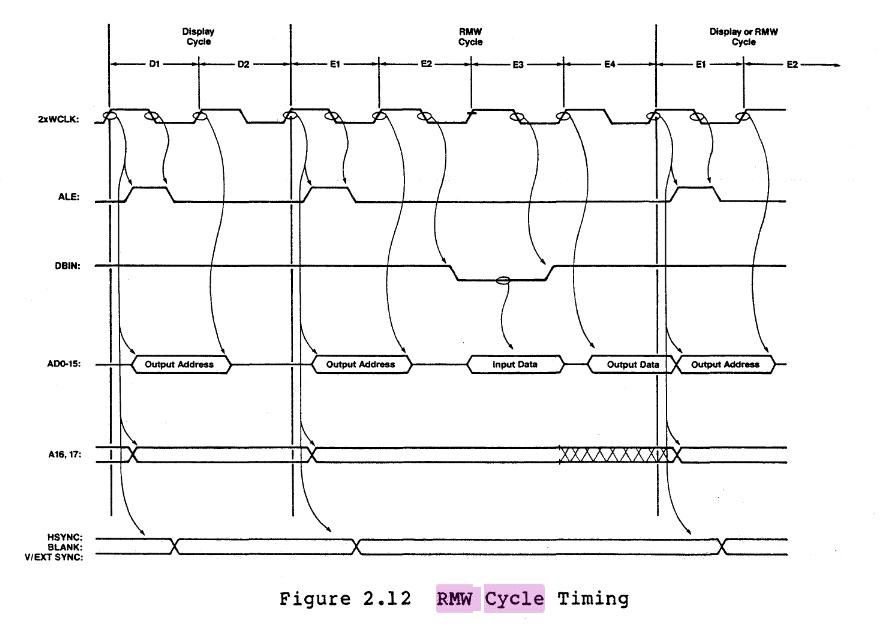 This image details the cycles of various uPD7220 memory accesses, and is super useful for designing the memory control logic.
Discussions
Become a Hackaday.io Member
Create an account to leave a comment. Already have an account? Log In.