What is it?
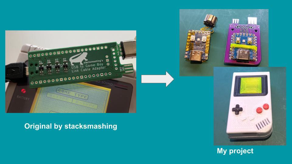
In a nutshell: I've made my own version of @stacksmashing's Game Boy Link Cable, or should I say in a GameBoy shell.
Features
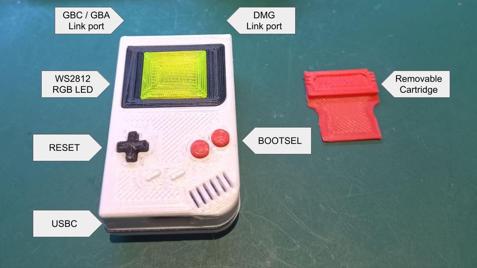
- USBC port - to connect to a PC or Phone.
- GBC / GBA / DMG Link port - auto select voltage for the level shifter 3.3V / 5V.
- Functional Dpad and AB Buttons - RESET and BOOTSEL respectively.
- RGB LED - visible through the translucent "LCD" screen, color change possible via BOOTSEL button.
- Removable Cartridge - a Game Boy isn't complete without game cartridges :)
Reimplementation
After watching the YouTube video by @stacksmashing on Online Multiplayer on the Game Boy. I got really excited to play my favourite game over the internet.
I was too late to get my hands on PCB from stacksmashing. In the mean time I noticed the components were dirt cheap on AliExpress. The RP2040 -Zero, an RPI pico alternative, caught my eye. This small board allows me to make a small Game Boy Link Cable.
After making my first prototype, I was not happy how fragile my construction was and I wanted something more sturdy.
Prototypes
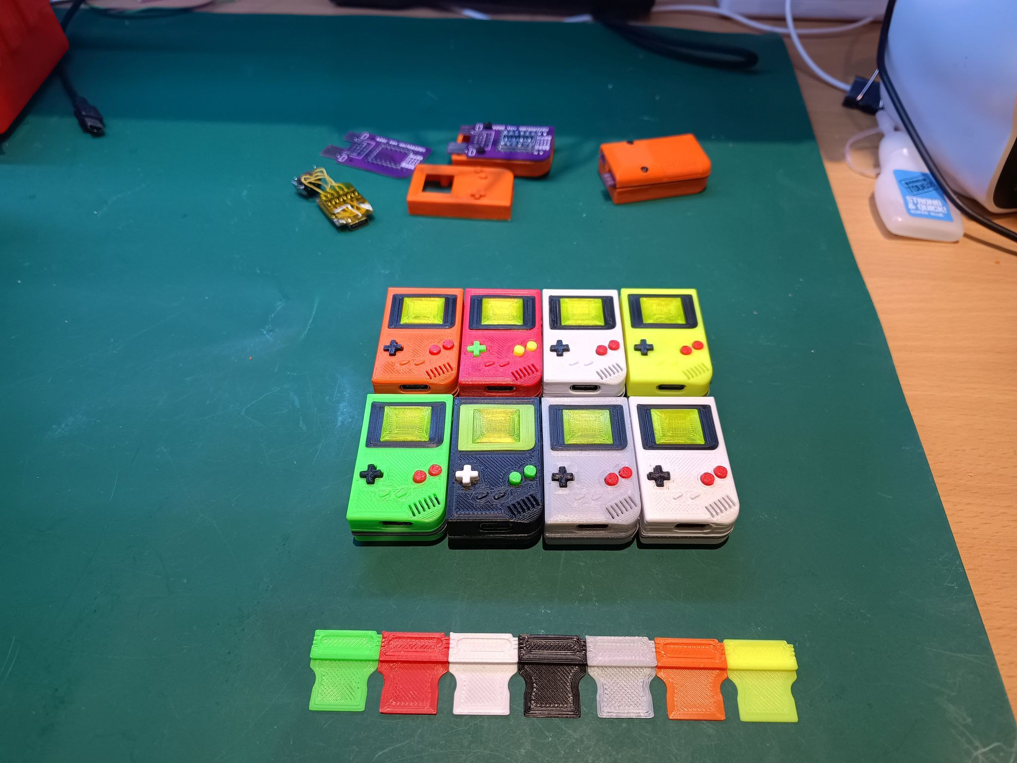
Here is an overview of the various prototypes I’ve made. I heavily relied on the “rapid prototype” philosophy on the modeling of the case. I’m a novice at 3D modeling, so there is a lot of trial and error in my journey.
Wired prototype
All the way on the left, is my first prototype. I just wired the RP2040-Zero and Level Shifter PCBs together. The original firmware worked and the assumptions I made based on photos and Firmware comments seemed to be correct. I liked the small form factor and I started to wonder if I could put some effort and make things nicer…
PCB Design
I struggled to get the Firmware to compile and I joined stacksmashing discord server. I found out about the PCB clone project by agtbaskara. At this moment I’ve never used Github and I’ve never used KiCAD before. Both were very pleasant to work with, I love the opensource nature where I can just fork projects to jumpstart my own. After a rough component placement I thought it might be nice to shape the PCB to the Game Boy itself with a nice rounded corner where the speaker goes.
Case Design
As mentioned before, I’m a novice at 3D modeling. I’m on FreeCAD and find that the learning curve is pretty steep. Good thing there are loads of video tutorials to guide and explain the tool and techniques. At first I wanted to keep the case design simple: just a top-case and a bottom-case in PLA which sandwich the PCB in between held together via two M2 screws. I went through 4 prototype stages.
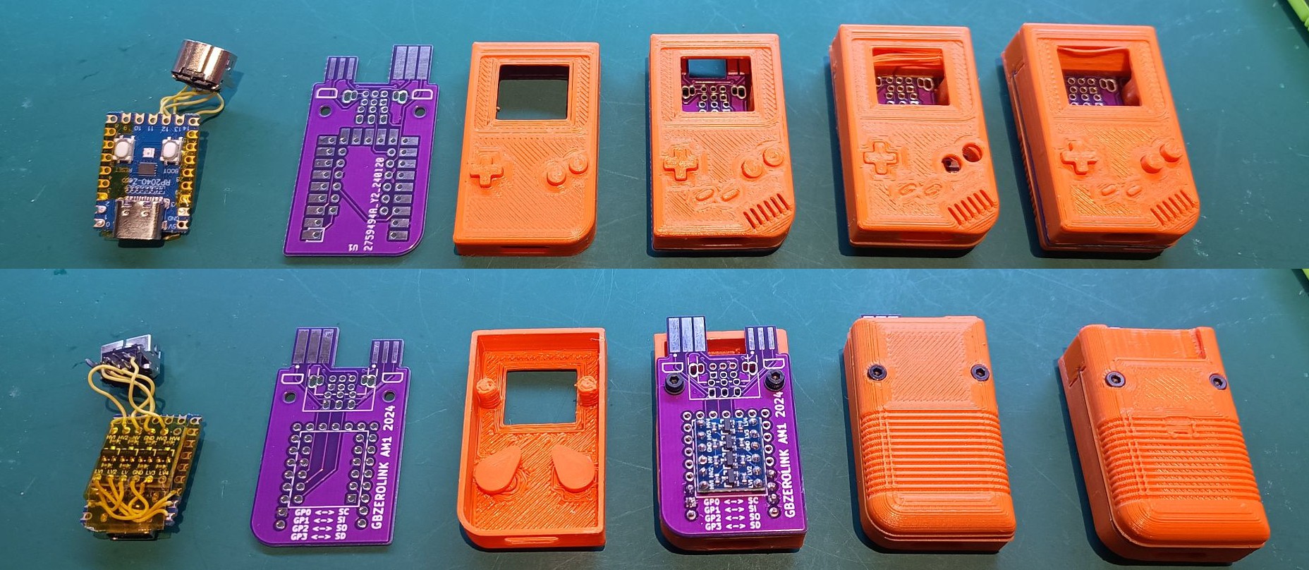
Case prototype 1) Started with the top shell. I wanted to make sure that my CAD dimension matches the PCB outline. Get the basic features of the Game Boy, like the screen and buttons. Trial out the shell thickness and see how the model looks coming out of my 3D printer. My print orientation is to finish the top on top, so I have to enable support for the print.
Case prototype 2) Previously I screwed up the screw post. I’ve made the screw post and the shell beefier. This time I’m able to screw down the PCB. I’ve modeled some extra details for aesthetic reasons, like the start-select buttons and the speaker grill with the slope cut off. In prototype 2 I wondered if I could keep the buttons of the RP2040-Zero still functional, despite that the buttons don’t line up perfectly under the Dpad and AB. So I modeled the Dpad and AB. The Dpad sort of worked, it was able to actuate the button, but at a weird angle. The AB just pivots in its socket and is unable to press the button. I’ve done a few iterations of the Dpad and AB buttons to get the height. A set of shallow buttons made its way to prototype 1.
Case prototype 3) An attempt was made to further improve the buttons by adding a wall around the button insert, such that it would “guide” button-travel downwards. This button-wall was actually interfering with the RP2040-Zero board. Furthermore, the bottom case was modeled. Initially just the bare minimum with some groves. I liked the details and I wanted to put more effort into modeling the details. The two part case does have an ugly discontinuation around the link ports…
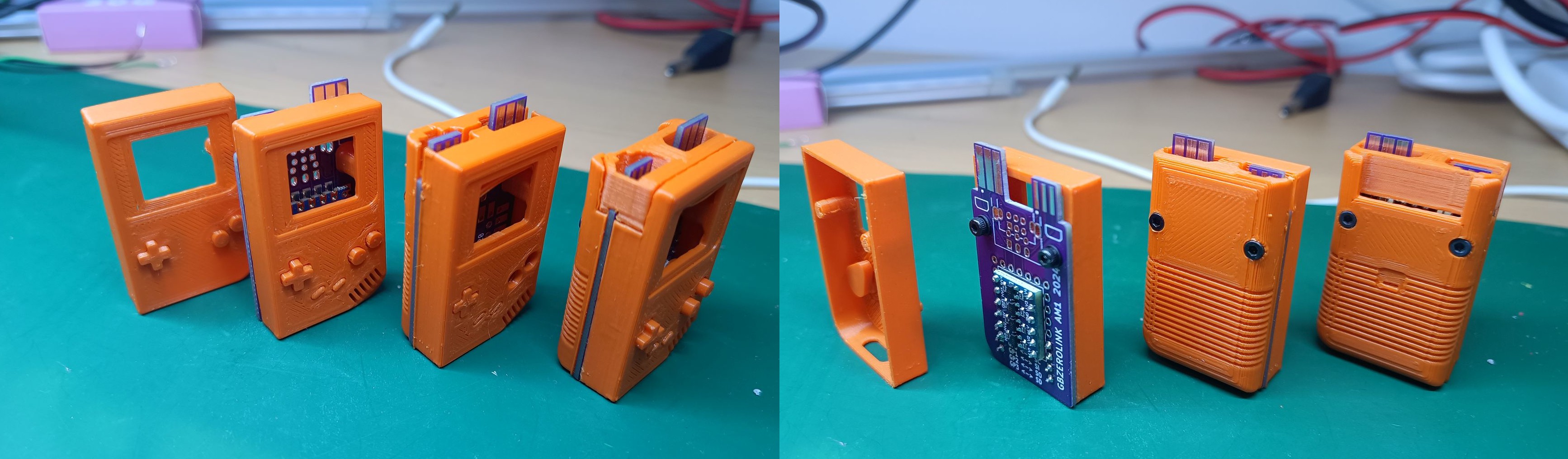
Case prototype 4) During prototype I stopped increasing the major version and went with increasing the minor version. I think I went all the way up to version 4.6. For the case, I settled with a three part design. The third part forms the link port housing. I managed to figure out a sort-of-ok solution for the buttons. It relies on a small plastic clip that acts like a pivot point for button to redirect button press. I really enjoy modeling the small details of the Game Boy and seeing these being printed out. I spend some more time on adding the batter clip. At this point I also added a cartridge. A few iterations later and I’ve got a removable cartridge system, you know, just for fun.
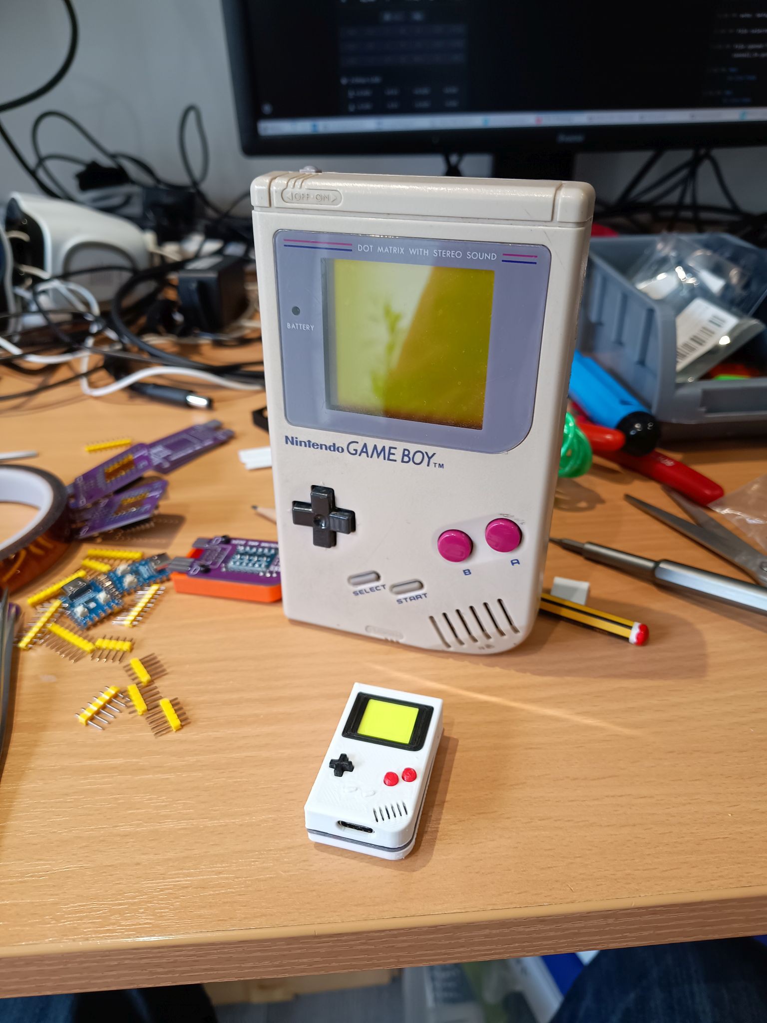
LCD Screen) The last challenge was to do something with the RGB LED that is present on the RP2040-Zero. I have this translucent neon-yellow PETG plastic. Being translucent I thought I would be able to print a lightpipe of some sort. Eventually kept it simple and printed a thin shell. The yellow is close enough to the original LCD screen and it is still able to show some the RGB light through. Which is good enough.
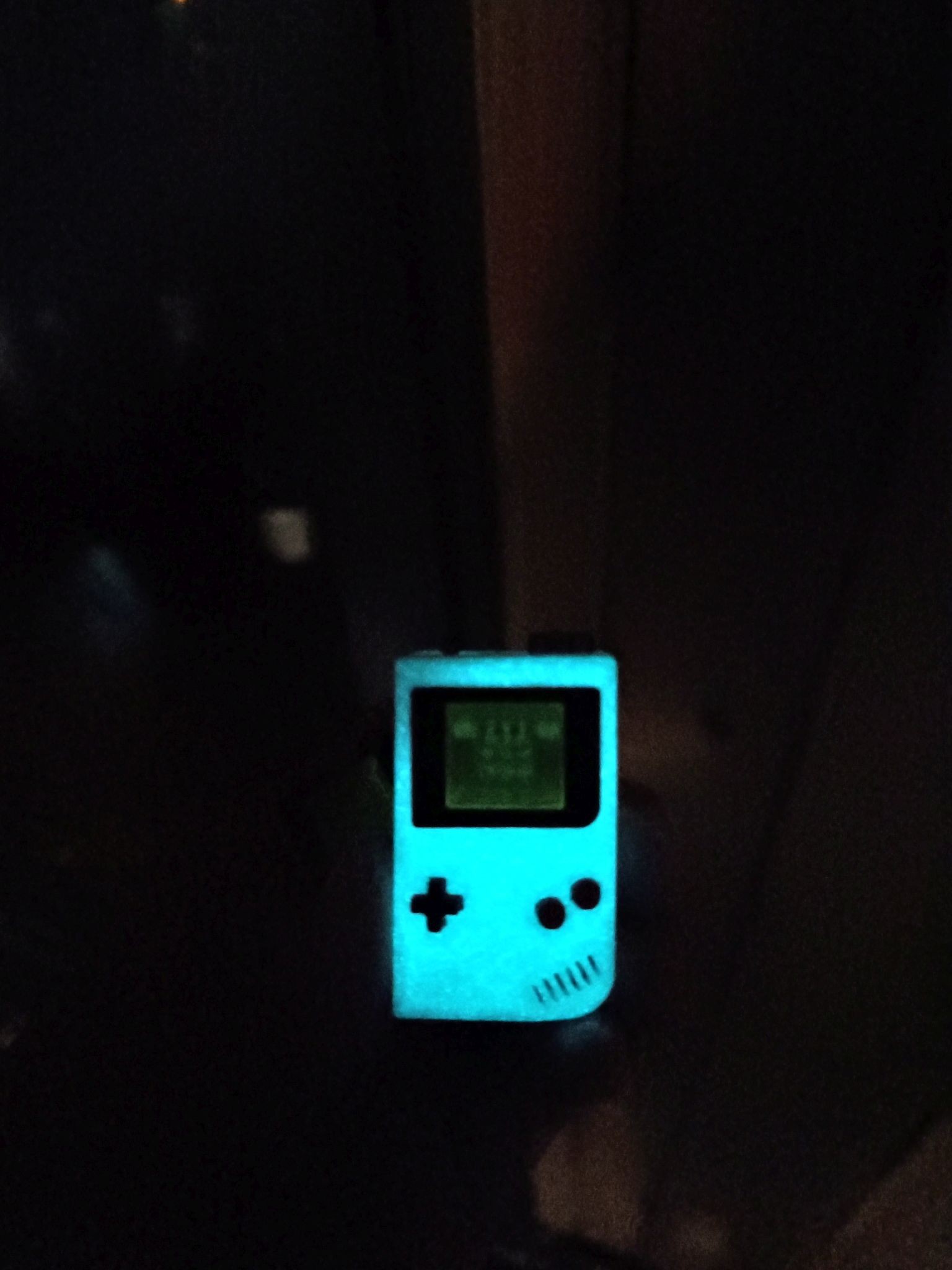
Glow in the dark
A friend of mine shared his spool glow in the dark PLA, so... why not :)
Credits and thanks
Thank you all for sharing your project publicly.
stacksmashing - The original Game Boy Link cable
agtbaskara - PCB reimplementation
Lorenzooone - Firmware fork that fixes tiny usb issues
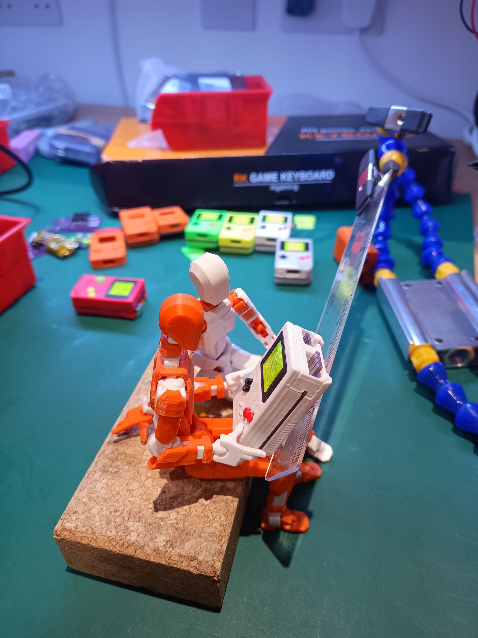
dummy-13 - figurines below depicting a typical scenario of my brother and I playing on the Game Boy <3
ttps://discord.gg/YASkVQY5Pr - stacksmashings's Discord server