 Dave Collins
I wanted a low cost kit like computer based around the 6809, with a very simple expansion bus.
Design goals:
- Cost - try to keep board footprints small (this was hard, further minimization with surface mount parts would be the way to go even lower)
- Minimal - keep the focus on simplicity, very few chips and very simple memory map
- Extendable - break out as many test points as practical and in locations that make them easy to bodge to.
- Runs existing firmware - Since I plan to use this as a learning platform I want the computer to be built around a reference design
- Grant Searles Page : http://searle.x10host.com/6809/Simple6809.html
- Jeff Tranter's page : http://jefftranter.blogspot.com/2019/01/a-6809-single-board-computer.html
- Open hardware (CERN-OHL-P) -- a text copy is in the files section if this link is ever bad.
Liability / warranty language from the license
5.1 DISCLAIMER OF WARRANTY -- The Covered Source and any Products are provided 'as is' and any express or implied warranties, including, but not limited to, implied warranties of merchantability, of satisfactory quality, non-infringement of third party rights, and fitness for a particular purpose or use are disclaimed in respect of any Source or Product to the maximum extent permitted by law. The Licensor makes no representation that any Source or Product does not or will not infringe any patent, copyright, trade secret or other proprietary right. The entire risk as to the use, quality, and performance of any Source or Product shall be with You and not the Licensor. This disclaimer of warranty is an essential part of this Licence and a condition for the grant of any rights granted under this Licence.
5.2 EXCLUSION AND LIMITATION OF LIABILITY -- The Licensor shall, to the maximum extent permitted by law, have no liability for direct, indirect, special, incidental, consequential, exemplary, punitive or other damages of any character including, without limitation, procurement of substitute goods or services, loss of use, data or profits, or business interruption, however caused and on any theory of contract, warranty, tort (including negligence), product liability or otherwise, arising in any way in relation to the Covered Source, modified Covered Source and/or the Making or Conveyance of a Product, even if advised of the possibility of such damages, and You shall hold the Licensor(s) free and harmless from any liability, costs, damages, fees and expenses, including claims by third parties, in relation to such use.
Support the Project:

10% of your order will go back into covering the cost of prototyping, parts and other materials for creating new and interesting projects for me to write about. Including new modules for the HB6809
Launch Video:
Build Files:
Github -- My Github for the HB6809
Build Recommendations:
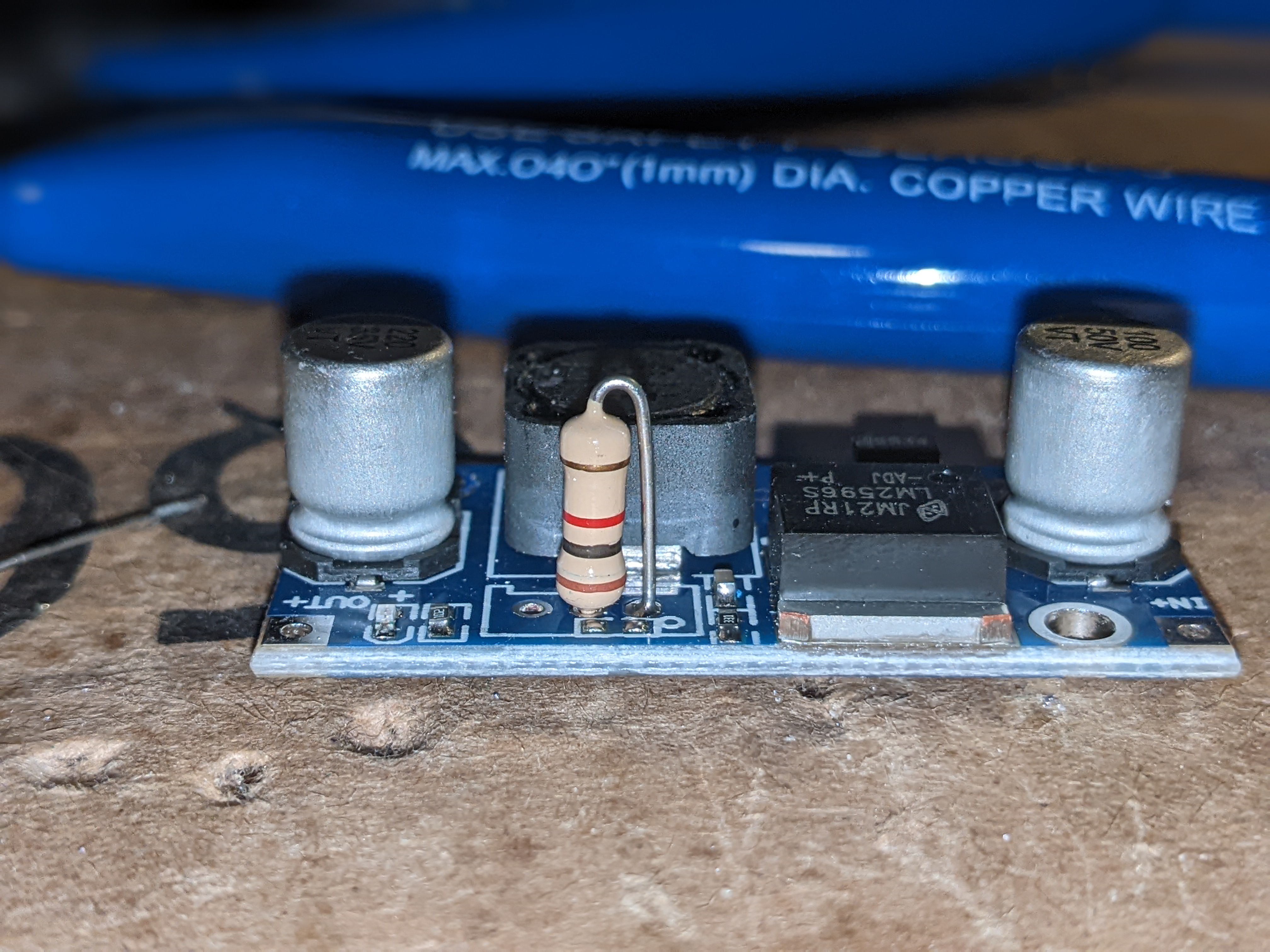
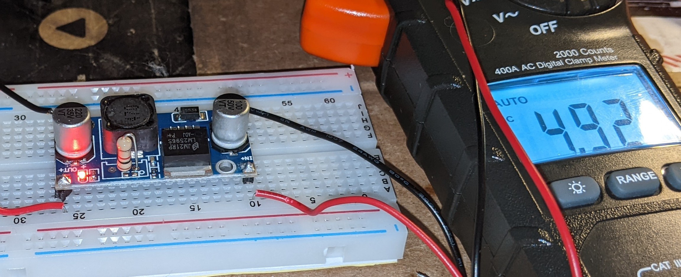
For the LM2596 DC to DC Converter module, It may be prudent to put break away pins (like used in a standard header ) on each of the four corners to prevent the module from shorting on the board. Additionally if you choose to remove the variable resistor from the module I found a standard through hole resistor (1K %5) provides a near perfect 4.9V you can simply mount it in the two holes that are laterally located next to the SMD pads that are revealed when you pull the variable trim pot from the board.
Optional power module mod:
Stand offs installed to prevent board from shorting:
HCT vs LS considerations:
I've used HCT logic chips in my design, you can build this with LS, but the fan out implications are considerably more dire. particularly with the address decode lines being tied directly to the two 74 series chips. Pay particularly close attention to the 6809 datasheet in this area, remember, HCT gates draw considerably less current from the bus, and since these decode gates are directly connected to the bus this will change those characteristics drastically if LS is used. Additionally It might be a good Idea to use bus transceivers on any expansions made for the system, to place the whole module in cut off unless it is being accessed, even one more module beyond the ACIA module this may be necessity; additionally these transceivers will allow the use of more modern HC or CMOS levels electronics on the expansion side of the interface which will in turn bring the total build current further.
Reset circuit:
This is a fairly simple tried and true RC Reset. Replace it if you want with a discrete one there is certainly enough space in the location of the reset pin for one of those three pin ones. The electrolytic cap is drawn to show polarity on the cap A tantalum / ceramic cap would be best, I did use an electrolytic, which is working more than fine for my build.
Switches:
The switch footprints are slightly off for the more commonly available 6x6 push button and 7x7 dpdt toggle. You can splay the legs out to make them fit, I did test this on the build to see if it works, and no issues thus far. Just be aware there may be more configurations than fish in the sea, and absolutely check the switches before soldering down, both should be normally open (disconnected when un-latched or not depressed)
Jeff's Firmware:
Please consult the HB6809 GitHub for recommendations on burning the eprom (TLDR; the start of the physical ROM must be C000h in the .HEX file, your offset should be C000.) The ROM on Jeff Tranters GitHub is here. You can also download a updated ROM with the expanded work area from the HB6809 Github. You can also use a 32k Electrically erasable eeprom the W27E257, or the D26256 by simply writing the rom data to the ROM starting at 0x4000
Serial Module:
You must mount the module in A000 for Jeff Tranter's Combined ROM to work. When building the serial card position the right angle connector to come out of the back of the board (in order for the pins to line up):
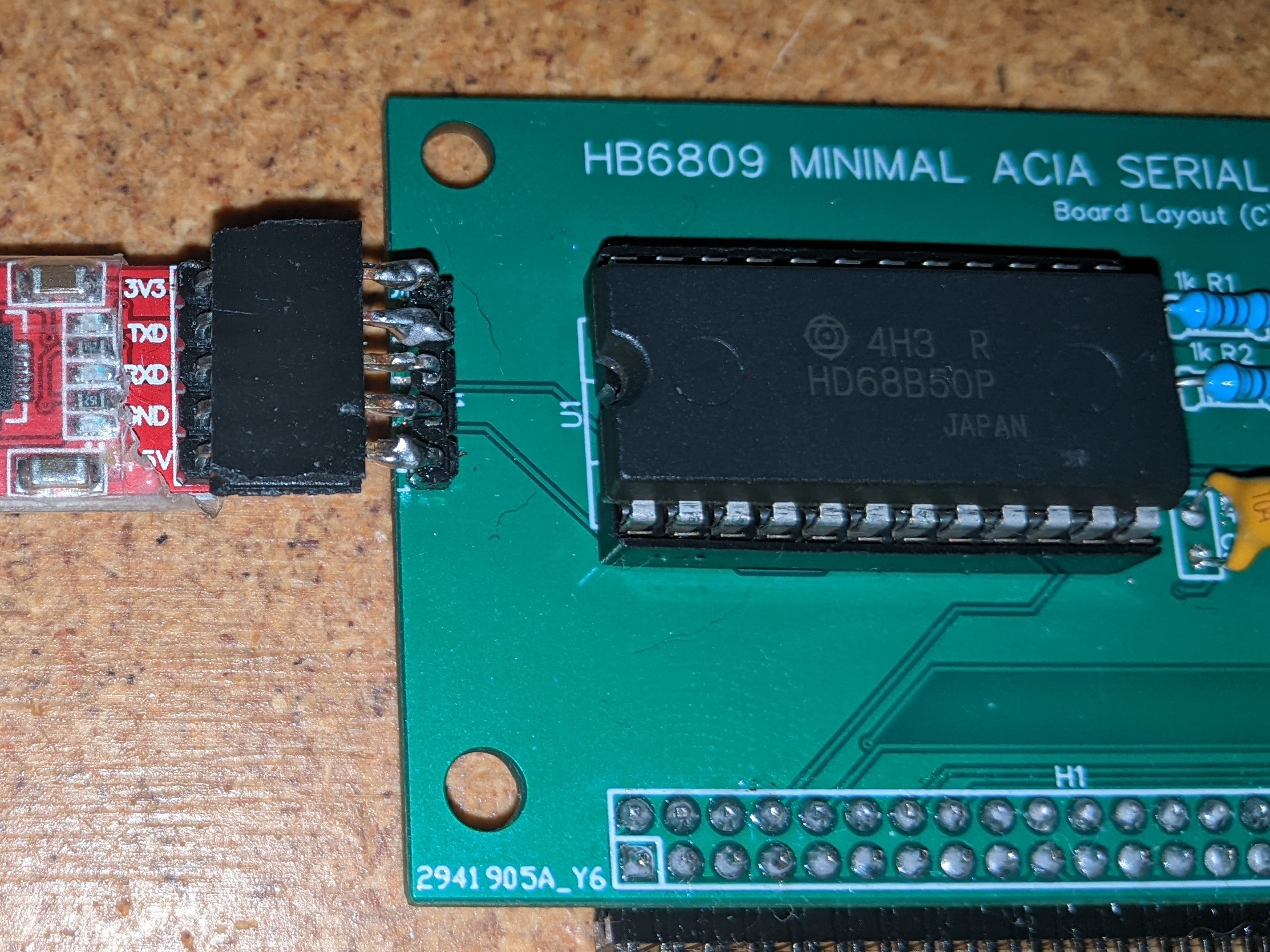
Also note the position of the TTL to USB link connections, they may differ on your USB link. ALSO 3.3v and 5v are not connected to anything here, only GND RXD and TXD are connected; you MUST bring power to the build via the power module (or bodge a link from the serial card to the bus -- not tested).
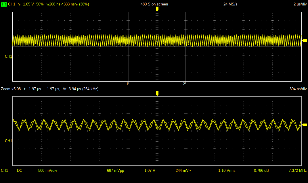
Default Scope Scans when at the Assist9 ready prompt:
found in the GitHub Here
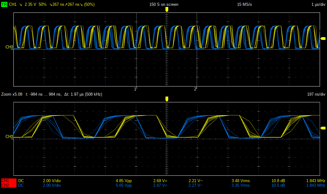
CLK (tests the main clock oscillator) :
E (tests the internal clock generation circuit ) :
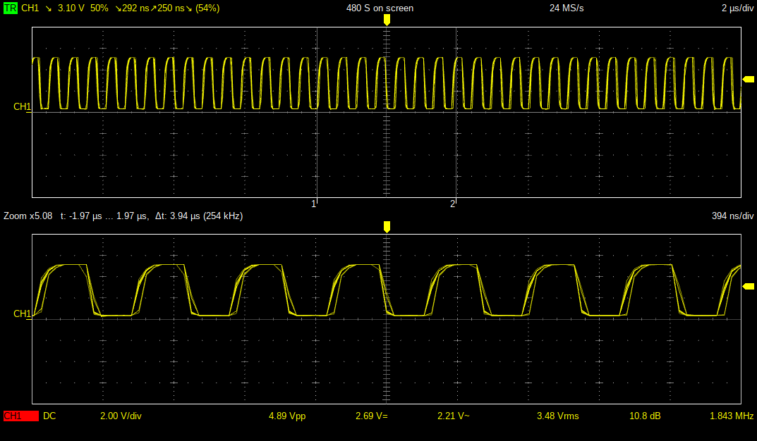
E&Q (more generation tests):
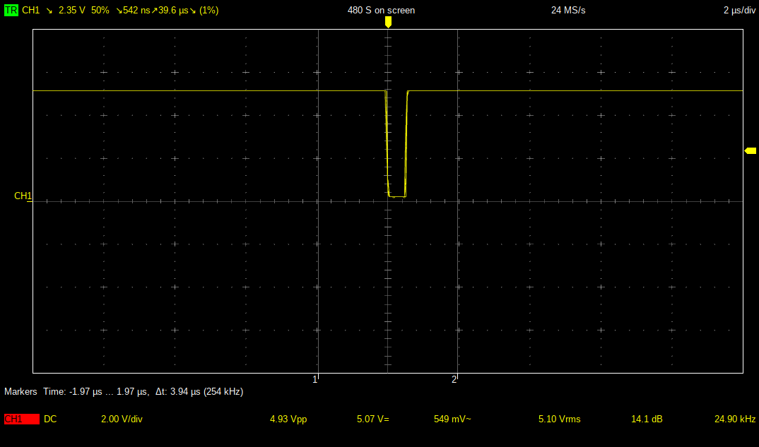
R/W (shows if the computer is at the ready prompt ) :
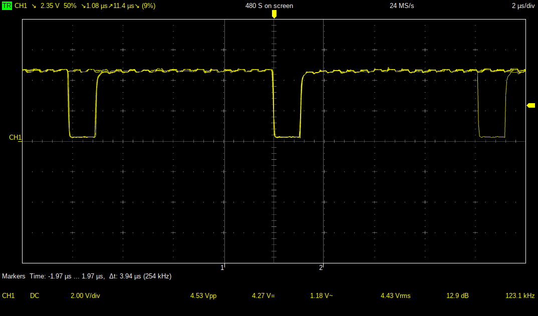
A000 (Tested off the decoder chip line -- another way to verify the ready state)
Some Housekeeping:
In case it's not obvious, I am not an expert. I am a hobbyist who really likes retro computing, programming 8 and 16 bit CPU's and designing and writing about these projects. I really would like it to be clear, though I do have extensive skills in this area, I am an autodidact. Everything create here, may be and probably is wrong in some way. Though I go through a lot of work to make sure it performs the way I would like it to, I don't think anybody should look at my body of work as a guide to "do things correctly". Additionally, I don't think I'm qualified to teach people about these things or really hold a valid engineering opinion on the "correct way of doing things." I do have a fair bit of, practical, and certified training in reading instrumentation, soldering, basic electronics, electrical work in general and networking. However at the end of the day I am an amateur, and you should take everything I say with a grain of salt .
All that being said, I really do appreciate the people who've helped me, and brought me to this point. If anything I make is successful its after a great deal of inquisition, research or outright generally coping what's worked for thousands of students, hobbyists and actual engineers.
The point of all of this is that this project is 100% as is, use at your own risk. I have verified this in my own home and do take a lot of care researching and asking questions about my designs. Everything I build is developed in a public forum of people who are smarter than I, for certain; this does not mean I can certify that these things are correct or free from defects. As with all things please use a great deal of caution when experimenting with these things, spending money on parts, PCBs and vintage chips.
Lastly, since this design is on the curtails of hobbyists and engineers who are far better and more experienced than I. That being the case I don't intend to sell, or profit from the HB6809 in any way, now or in the future. I do plan on providing all the source materials for free (just as Grant and Jeff have done before). I don't take credit (and won't for that matter) for the great work that they have done before me. It is very important to me that others can try out and play around with these designs. To that end everything is going to be 100% open hardware, and freely available so that anyone can download the designs and build a computer of their own.
All that being said, PCBWay has kindly offered to do the fabrication on the last set of PCB's for this project, in an exchange for a review of the quality of the boards; which I am happy to do as I have always been very pleased with the quality of their services. PCB's are expensive and this really has become a major passion project for me. Without the help of sponsors like this It would take ages to Finnish a project that may only see a few copies in the hands of people who are truly interested, and so to me it is worth it to accept the assistance, especially since the aid is only in services rendered (and contains no monetary gain for myself) and directly benefits finishing the project.
Additionally this entire project is being released as open hardware under CERN-OHL-P and the layout is copywrite David Collins 2022