 Eddie
EddieWith TeeEye I used an optocoupler for each character that I wanted to type. This came out to around 30 optocouplers/IO pins that were needed. Scaling that up to 150 devices would be over 4000 optocouplers. While this would be visually interesting (and something I would love to do) I decided to search for a more efficient/scalable solution.
Here is an article on how keypads work since that's outside the scope of this document but essentially when you press a button you're connecting a point at a column and a row which in my case is interpreted but the device's internal brain and displayed as a character on the screen.
My friend Freakylampss told me I should try using a multiplexer so that's the direction I decided to pursue!
With this information, I was able to come up with a solution that could use a shift register along with a multiplexer/demultiplexer to control every button on the device! Effectively taking the previously needed 30 IO pins down to just 3. This would allow me to control six screens from a single Arduino!
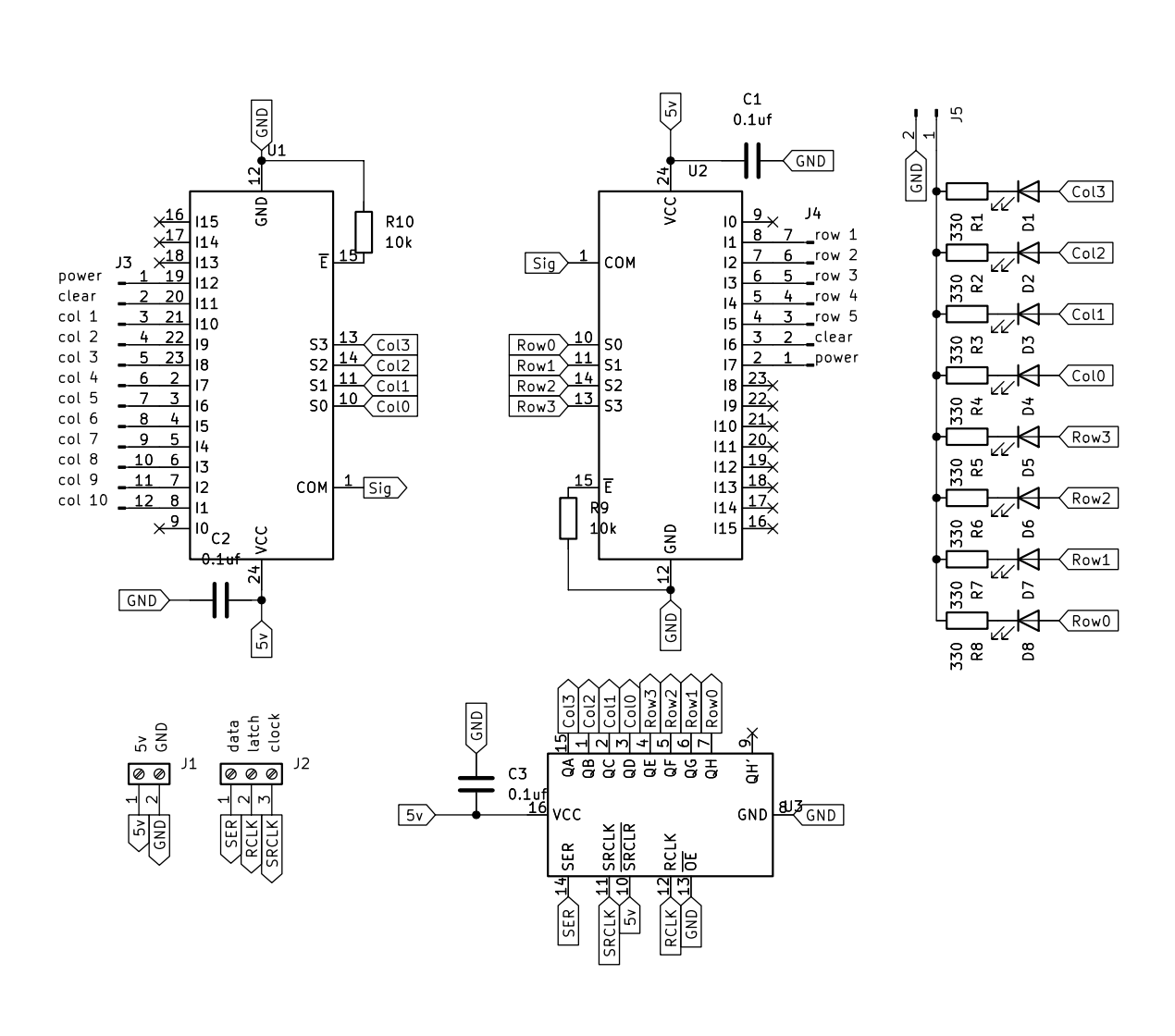
Below is the schematic for the circuit that I ended up using.
Here is a list of links/tutorials that helped me figure out what I was doing after my friend sent me in this direction as well as information on how multiplexers and shift registers work.
Multiplexer - How To Guide (The guide is for a different chip but the principals are transferable)
Shift Register - Tutorial from Arduino website.
So how does the circuit work?
The Multiplexer/Demultiplexers each take a 4-bit number that is used to select an input pin on the multiplexer and an output pin on the demultiplexer. I took these two separate 4-bit numbers and created a single 8-bit number. I can then use the shift register to send out this single 8-bit number with bits 5-8 controlling the multiplexer and bits 1 - 4 controlling the demultiplexer.
I then just needed a way to know what 8-bit number I needed to route the signal so that a button press could be emulated.
I made the following table to help get all of that information sorted.
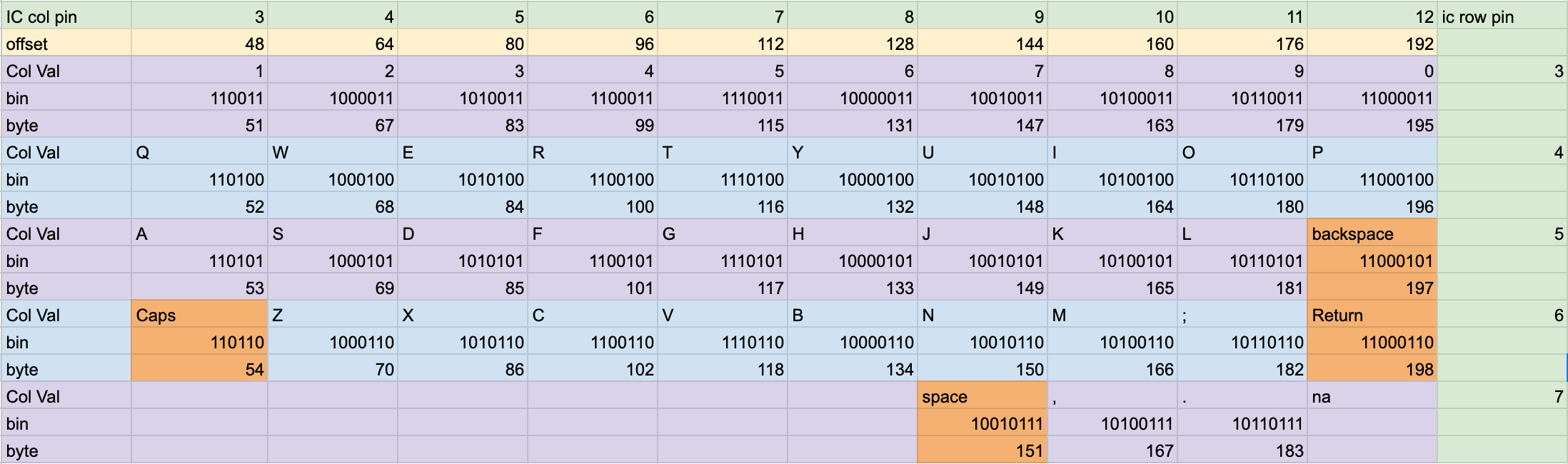
IC col/row pin is the pin assignment on the multiplexer and demultiplexer
Col Val is the value that should be typed on the screen when the column/row connection is made
bin is the binary number we send out to create a path between the multiplexer/demultiplexer
byte is the decimal representation of the binary number which I used later as a method of storing long strings of text without needing all the space that strings typically take up.
This process took some time to figure out and I felt pretty lost along the way but through trial and error, I got it all to work!
You can see the shift register sending out the 8-bit value and the multiplexer/demultiplexer on the right counting values. The lowest breadboard ended up getting scrapped in the final design which is why it's not present in the above schematic.
I think we can all agree that moments like this are why we're here.
Discussions
Become a Hackaday.io Member
Create an account to leave a comment. Already have an account? Log In.