 Jamie
JamieI intend on using the original GameCube power-on button to turn the PC on, however there is a slight problem. The documentation for the NUC states that the power on header must be pulled to ground for at least 50ms via a momentary SPST switch to turn the PC on/off. The GameCube switch is latching.
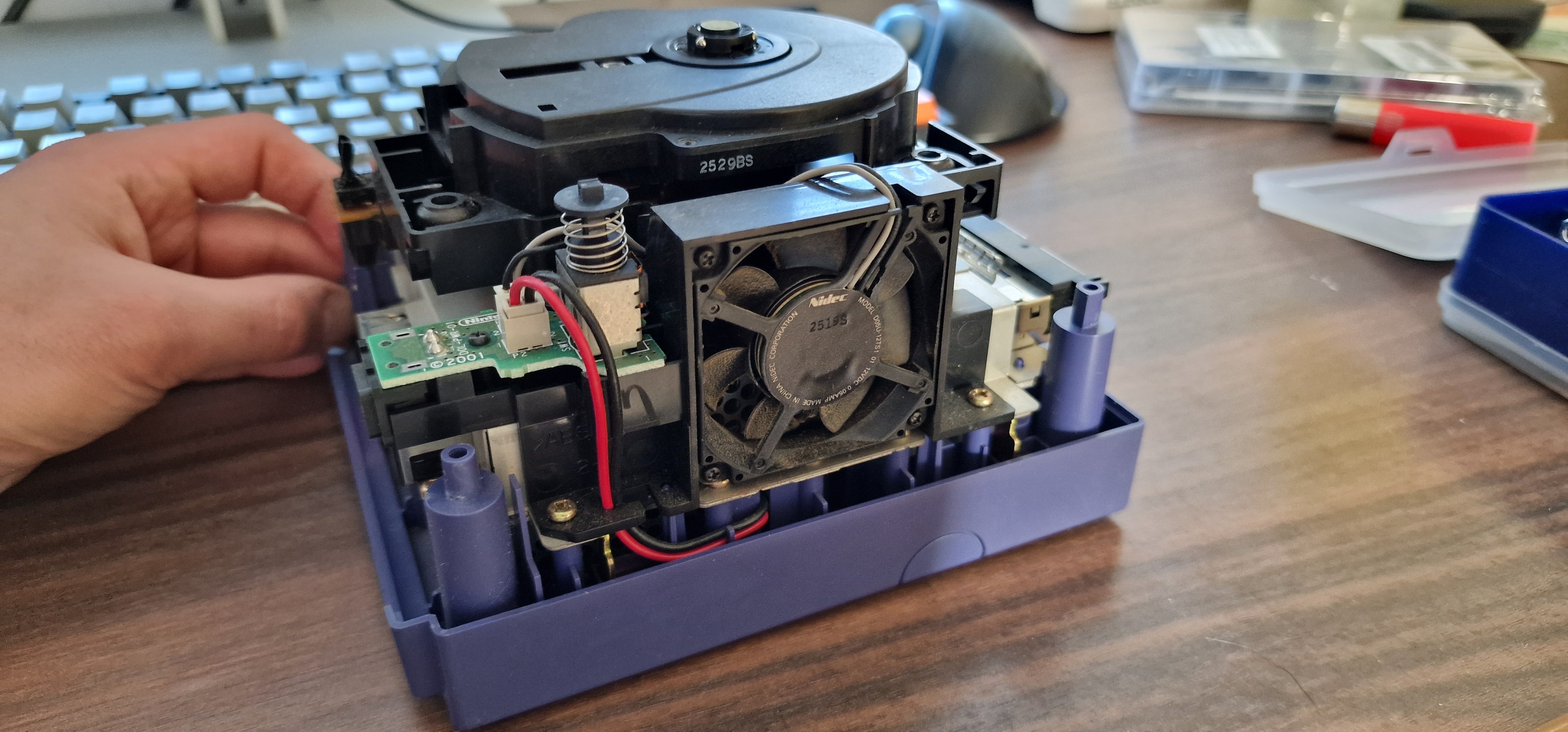
GameCube power switch on the fan assembly.
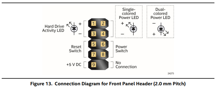
Front panel header pins.
I needed to find a way to detect when the switch state changes, and use this to generate a pulse that will allow pin 6 to be pulled to ground (pin 8) for a defined time period.
To begin with I considered a more "analogue" solution. From my research, I learned that a resistor-capacitor network can be used as a dual edge detector. This can then be fed into monostable multivibrator (such as with a 555 timer) which can then drive a relay, optocoupler or other transistor to enable current to pass. After a bit of experimenting and not much luck, I posted my question here where I received some great responses and help. I can't take much of the credit here, but this appeared to be one of the most promising solutions from my simulation:
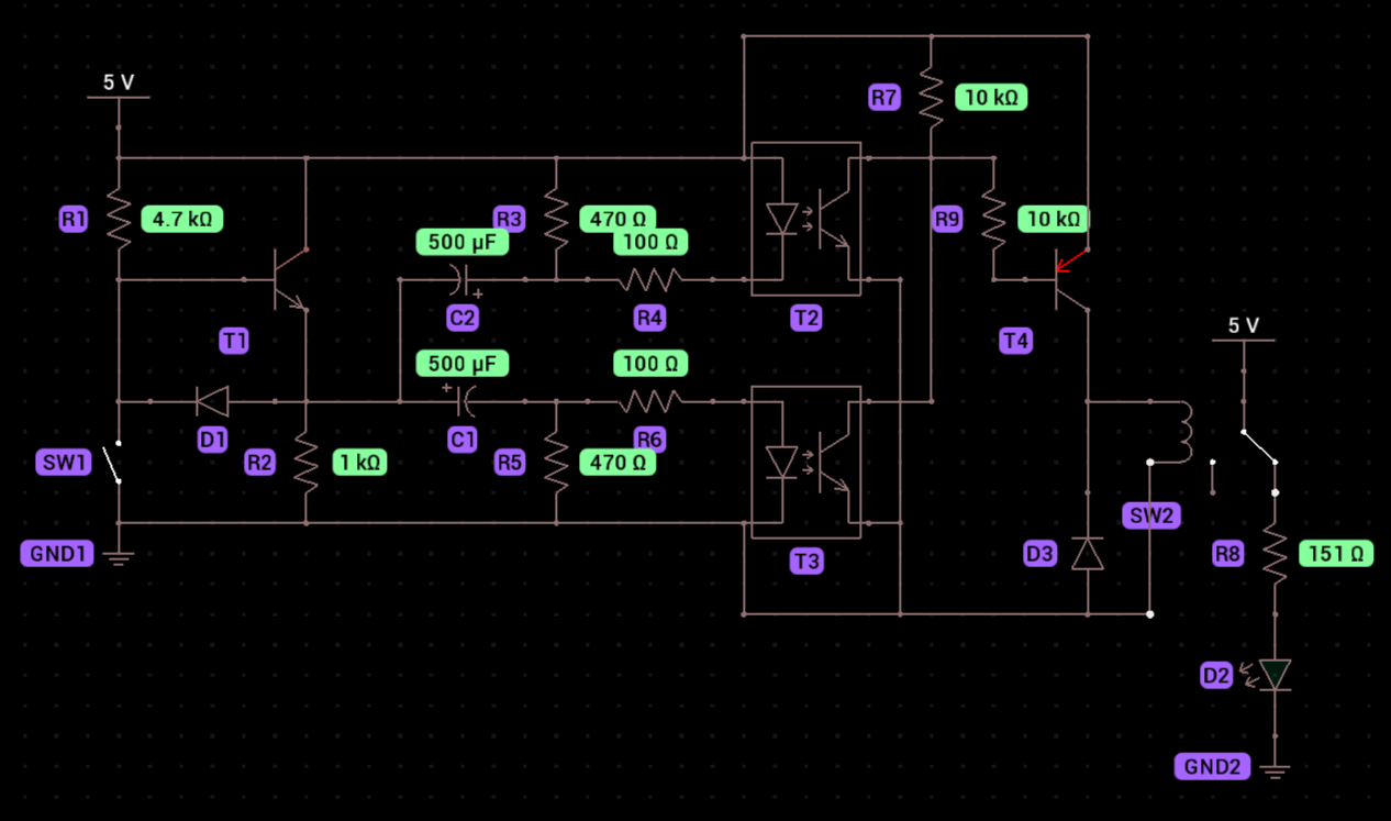
Here is a breakdown of how it works (I think?):
- When the switch is closed, 5V is pulled down to GND via R1 and the upper capacitor/resistor/optocoupler network (C2, R3, R4, T2).
- When the switch opens, the current goes through T1 instead. Because of diode D1, the current is forced to travel through the lower capacitor/resistor/optocoupler network (R2, C1, R5, R6, T3) instead.
- When the switch state changes, the capacitors discharge enough current to power the optocouplers. When they finish discharging, the voltage isn't sufficient to bypass R7 so it goes back to the steady-state pathway (the upper/lower networks on the left hand side) instead.
- When either optocoupler is powered, current flows through R7 which powers T4. This then allows current to pass through R9 to relay SW2. The LED and 5V connection on the relay signify pins 6 and 8 on the NUC.
It is worth noting that the size of C1 and C2 have the most impact on the pulse length. R3, R4, R5 and R6 have some effect on the shape of the pulse.
But, truth be told, I have no idea what I'm doing here and I'm well out of my depth. I decided to search for alternative solutions.
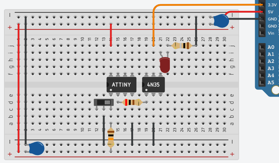
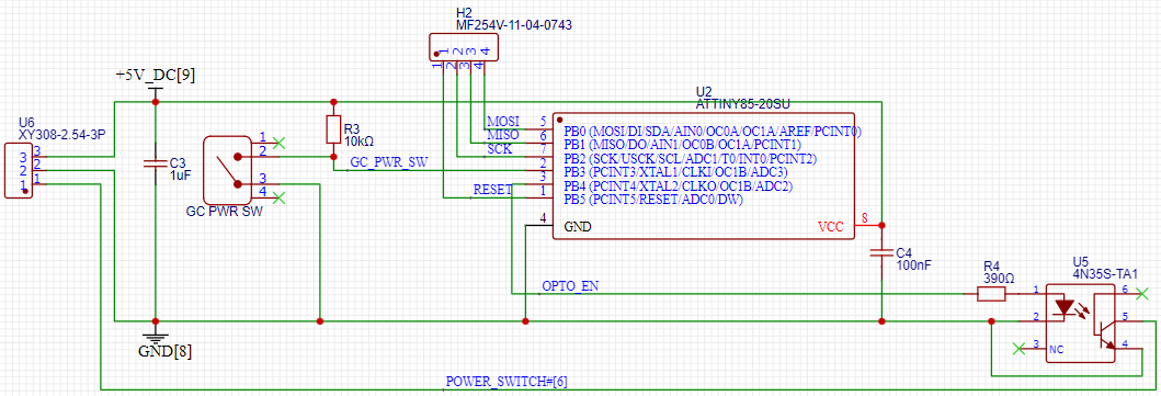
It was then that I learned about the infamous ATTiny85. I put together this beauty in TinkerCAD:
And, surprisingly, it works! Here's the breakdown:
- The ATTiny85 is powered by 5V from pin 9. The switch is connected between any one of the GPIOs (pulled up via a 10k resistor, in this case PB5 is used) and GND.
- A second GPIO (here it is PB3) is connected to a 4N35 optocoupler. When the switch state changes, a pulse is sent by the MCU to the optocoupler. This allows current to pass from header pin 6 (illustrated here as a red LED) to GND.
- The capacitors are for some basic filtering. Ideally, a 0.1uF cap will be placed close to the MCU's VCC and GND pins, and a 1uF cap close to the power supply.
- The ATTiny85 is programmed to do the following:
- The initial state of PB5 is recorded in a variable "lastSwitchState". PB5 is constantly monitored on a loop.
- When the state of PB5 is low and lastSwitchState is high or vice versa, a pulse is sent to PB3 for a set amount of time, then after this is done lastSwitchState changes.
- There is also a delay to programmatically debounce the switch.
const int switchPin = 3; // Pin connected to the switch (ATtiny85 pin 2, Arduino pin 3)
const int ledPin = 4;    // Pin connected to the LED (ATtiny85 pin 3, Arduino pin 4)
int lastSwitchState;     // Last stable state of the switch
unsigned long lastDebounceTime = 0;  // Last time the switch state was toggled
unsigned long debounceDelay = 50;    // Debounce delay to prevent noisy signals

void setup() {
  pinMode(switchPin, INPUT_PULLUP); // Configure the switch pin with internal pull-up
  pinMode(ledPin, OUTPUT);          // Configure the LED pin as an output
  lastSwitchState = digitalRead(switchPin); // Initialize the last known switch state
}

void loop() {
  int currentSwitchState = digitalRead(switchPin); // Read the current state of the switch

  // Check if the switch state has changed from the last read
  if (currentSwitchState != lastSwitchState && (millis() - lastDebounceTime) > debounceDelay) {
    lastDebounceTime = millis(); // Reset the debounce timer

    // Toggle the LED for 1 second if the state changes
    digitalWrite(ledPin, HIGH);   // Turn on the LED
    delay(1000);                  // Keep it on for 1 second
    digitalWrite(ledPin, LOW);    // Turn off the LED

    lastSwitchState = currentSwitchState; // Update the last switch state
  }
}
I ordered some parts on Amazon, and with the wonders of 21st century next day delivery, began prototyping. I used this really well written guide to help me program the ATTiny85. I almost squealed like a little girl when this worked:
As long as I don't try to bring this to an airport, I should be okay right?
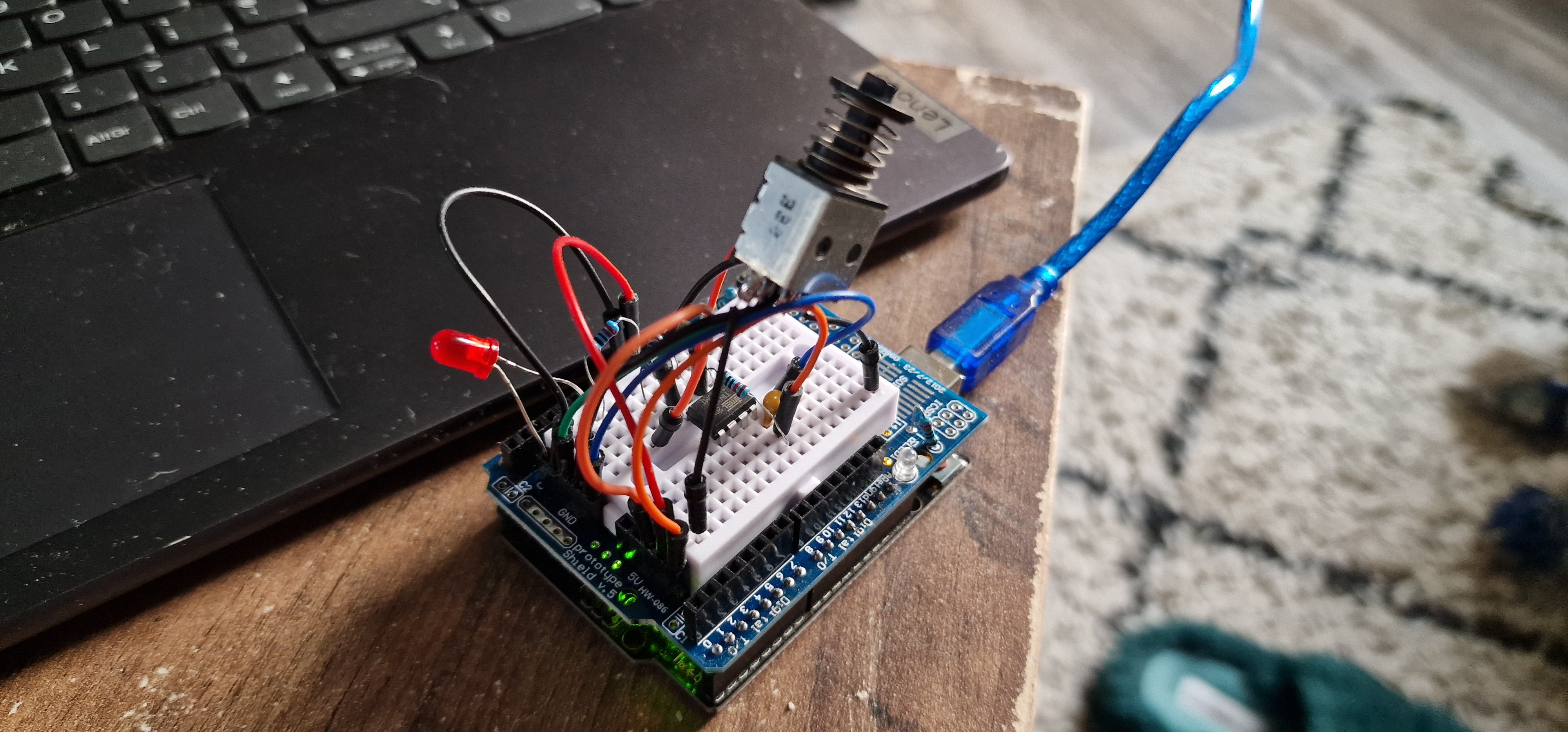
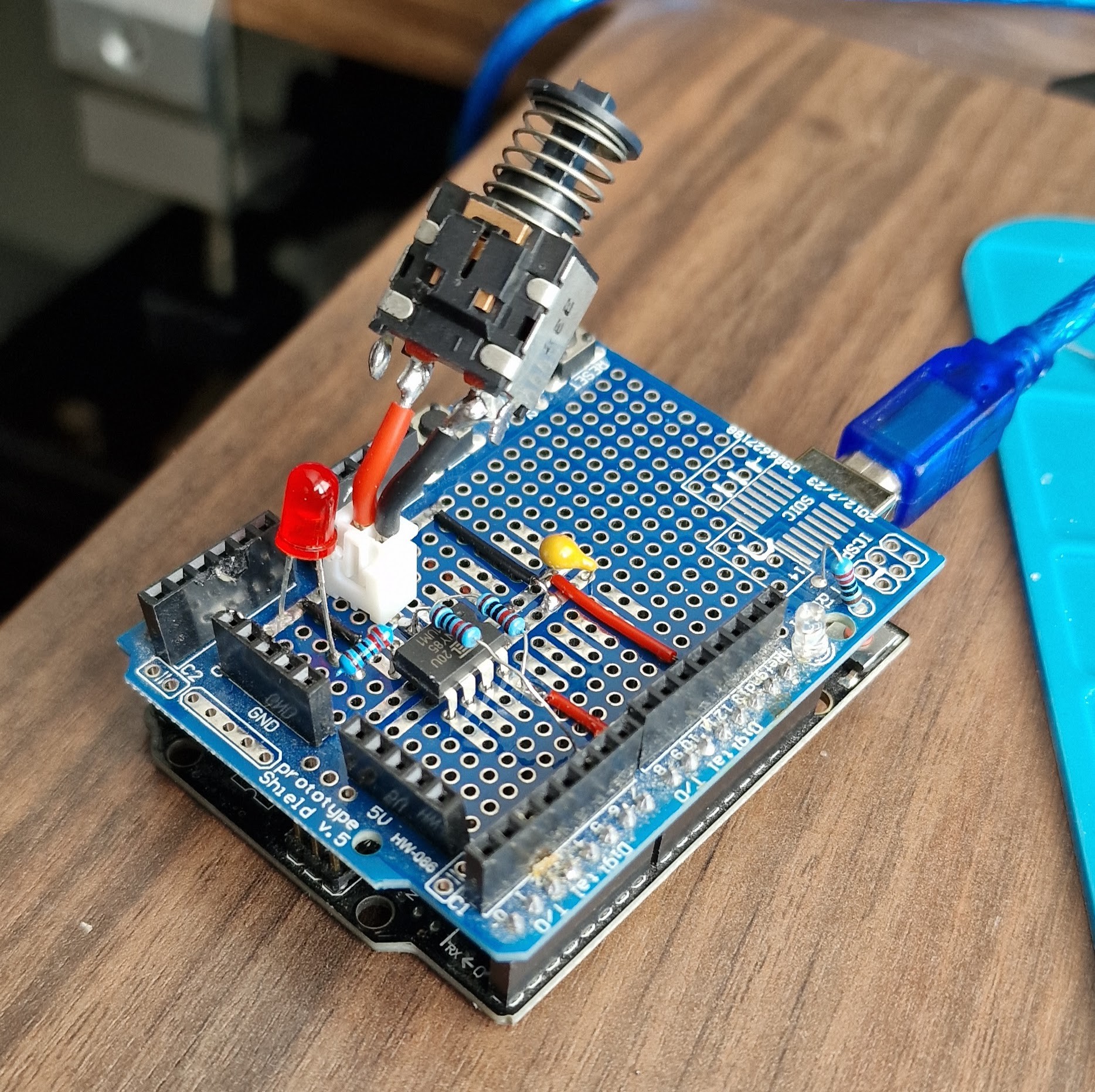
I had some issues with my jumper wires disconnecting so I prettied things up a bit:
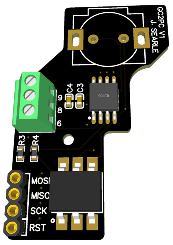
Now that the circuit appears to work, I began working on the PCB. I have never designed a PCB in my life. The thought of it was quite intimidating.
I decided I was going to use JLCPCB to produce my PCB due to their assembly service (I don't have a reflow oven or any feasible method of soldering surface mount components...) and the EasyEDA software which integrates seamlessly with their component catalogue and online quotation process to make life easy. JLCPCB, if you're reading this, please sponsor me, you won't regret it.
A few painstaking days of working out how to design a PCB later, I had revision 0:

Isn't she a beauty? It's worth mentioning I haven't been completely honest about the chronology of this process. I definitely did not get too excited early on and design this PCB and order it before working out where the +5V is grounded to, or before adding the aforementioned filtering capacitors.
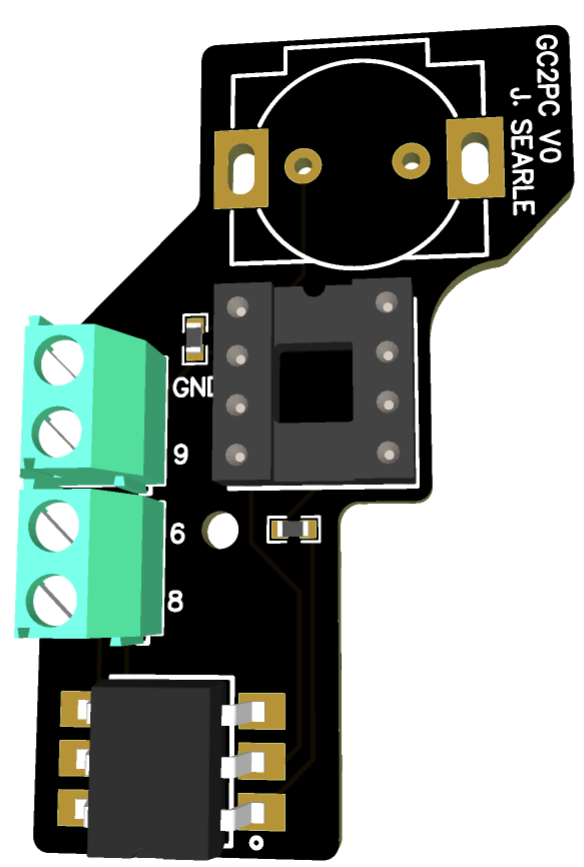
At first I decided to use an 8 pin IC socket to hold the ATTiny85 so I could program on the breadboard then transfer it across. But in hindsight this is a massive waste of space and adds no value. So I made some revisions:
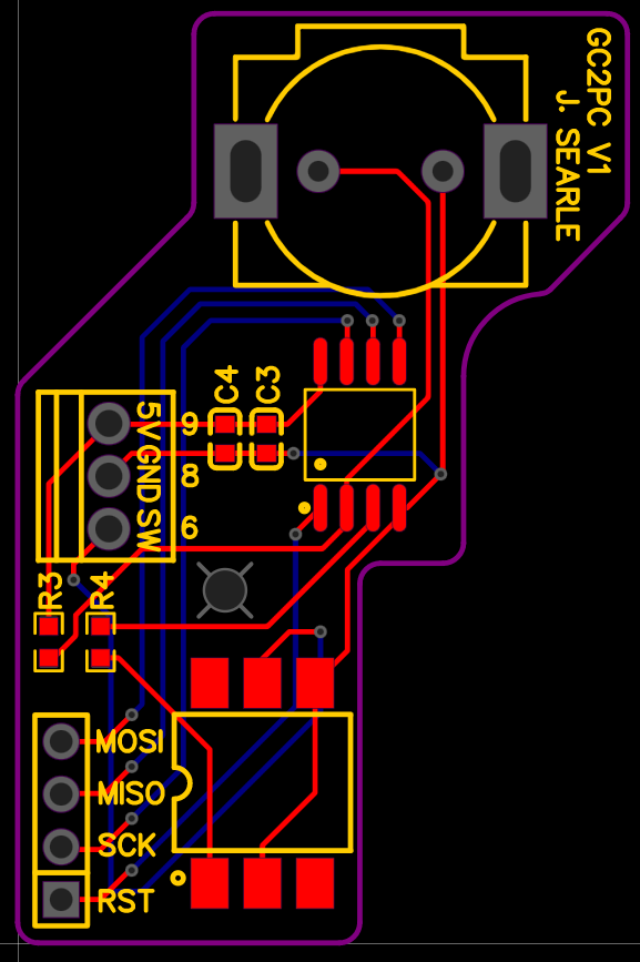
With the addition of the lower left hand side female headers, I am able to program the ATTiny85 directly on the PCB. I'm not sure how I feel about using circular pins though, I'm more of a square pin guy myself.
Excitement aside, I would greatly appreciate some feedback on the PCB and circuit design. The next step is to assemble V0 when it arrives and find out if the optocoupler will do it's job as that is the only part of the circuit that is currently untested. This will also give me a chance to make sure the dimensions of the board and component placement are correct. I'll then make any final changes to V1 (let's call it V1.1) and order the (hopefully) final PCB. I will be making all PCB files available when the project is complete so that anyone can build this themselves.
Discussions
Become a Hackaday.io Member
Create an account to leave a comment. Already have an account? Log In.