 ridion3D
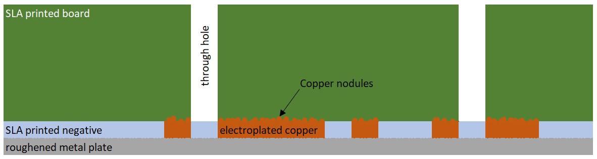
Disclaimer:
I abandoned this project over a year ago because of ADHD, anxiety and self-doubt. I'm only posting it now because I saw a post on reddit a few days ago that described what I'd done a year ago, and it made me feel sick that I hadn't published it then because I thought it was useless.
I haven't really documented anything back then, so everything I write here is from memory. And sorry if there's too much information, it was quite therapeutic for me to write it all down.
Start:
Over a year ago now, I needed a very simple PCB for a very simple project, but it had some surface mount components, so one of those through-hole prototyping PCBs wouldn't do. I could have etched a plain copper PCB the usual way, but I hate cutting and drilling them with a passion.
Since I had an FDM 3D printer, I thought I might be able to print a plate with channels for thin wires and then solder the components to the wires (pretty much like so: reddit). After a few attempts, I abandoned the idea because the heat from the soldering iron would damage the plastic.
The next thing I thought of was printing a board with the through-holes, then glueing a sheet of copper to it and doing the normal dry film, exposure, development and etching process. I also used a laser printer to print directly onto the copper, so I didn't need the dry film, which worked better than expected, but not that great.
This is one of the few images I have of an FDM printed board. It seems to be one of my earliest attempts. I think it was one where I laser-printed directly onto the copper, because of the black parts and the bad quality of the etching. Also aligning the copper with the toner transfered layout onto the plasic was hard.

Although it worked somehow, as my 3D printer obviously couldn't produce consistently good small holes, it ended up being more work than if I'd just drilled a normal PCB. It also had some other problems I can't remember. I printed it upright on one side instead of flat to get nicer holes, so it would also be prone to breaking along the layer lines.
I was then in this ultra-motivated phase where I really wanted to make it work. So I bought an SLA printer, thinking it should be able to print a perfect board with nice holes.
Since I had no experience with resin printing at all, it took a while and almost a bottle of resin to get a feel for it. It's pretty straightforward when you're printing larger things, but it's a bit trickier when you're printing holes as small as 0.6mm. Then bleeding and whatnot comes into play. Also the first layers need a longer exposure time to stick to the build plate, but this will make the holes smaller or close them completely.
It took a lot of time (and resin) to get consistently good results, but I was reasonably happy with it.
Copper Layer

My initial idea was to print the board with the through-holes directly onto a sheet of copper and then do the standard dry film stuff. So I ordered a roll of copper tape. It was a bit thin, but for simple prototype digital circuits it should be enough, I thought.
So I stuck a piece of the copper tape onto the stock build plate of my printer and tried to print the board onto it. As you can imagine, the resin didn't stick. I tried to make the copper surface rougher by sanding it. But it just didn't work. The sandpaper was either too coarse, so the thin copper would tear, or it just didn't do anything to the copper. The soft glue under the copper made it difficult. So I scrapped it.
The next idea was to just glue the copper onto the board like I did with the FDM printed PCB. I used some generic 5 minute epoxy glue. But here I had a similar problem. The copper wouldn't stick to the epoxy. Again I think because it was too smooth. I went through with the dry film and so on, and visually it looked great, like a real PCB, but it was far too easy to peel the tracks and pads off. ...
Read more »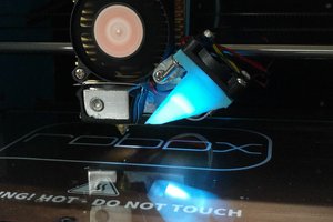
 Rob Ward
 fl@C@
fl@C@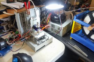
 AccidentalRebel
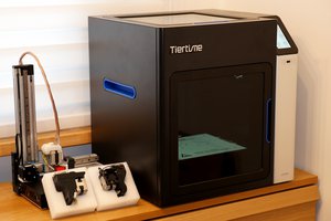
 megahercas6