Close
0%
0%

PCB Artwork and Photo Conversions

We'll be talking about how to do PCB artwork with Andrew Sowa

Friday, April 20, 2018 12:00 pm PDT Local time zone:
Hack Chat
Similar projects worth following

Join this Hack Chat by clicking on the JOIN HACK CHAT button. 

______________________________________________________________________________

Andrew Sowa will be hosting this Hack Chat. 

This Hack Chat is at noon Pacific time on Friday, April 20th. 

Time Zones got you down? Here's a handy count down timer!

Andrew Sowa is an electrical engineer with a background in circuit layout and LED lighting. He has been a vocal advocate of KiCad which he used to make two crowdfunding products and his own style of PCB art. Andrew has recently started sharing his past experiences on the SupplyFrame Hardware blog and his self titled Youtube channel. He was recently a guest on The Amp Hour!

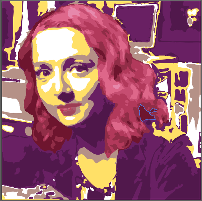
PCB Art is likely as old as the manufacturing process itself. It has evolved over time from engineers hiding easter eggs in wasted space to whole companies devoted to the intricate authentic design. Andrew has created his own style by using each layer of the PCB to make multi-color images from computer generated designs.  In this chat he will talk about his process of turning photos into PCBs as well as tricks to getting high resolution results with KiCad. 

TL;DR

In this chat, we'll be talking about PCB artwork:

  • Bitmap to SVG Converstion (Inkscape and Illustrator)
  • Kicad Footprint creation
  • PCB Fabrication Limits
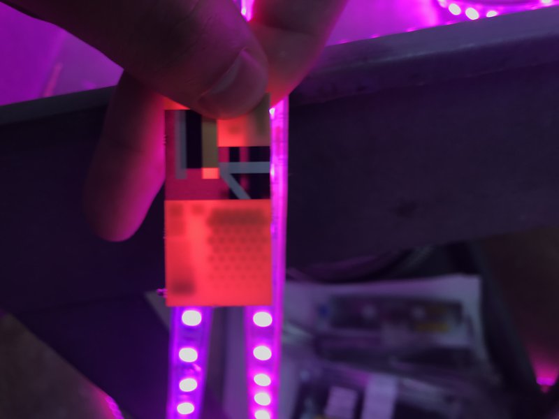
  • Backlighting
  • Halftones

View event log

Enjoy this event?

Share

Discussions

deʃhipu wrote 04/20/2018 at 19:10 point

Do you know of any PCB pixel art?

  Are you sure? yes | no

Robert Mateja wrote 04/20/2018 at 19:07 point

Is there secret 9 3/4 for chat or how to get in conversation? join hack chat button says

" THIS CONVERSATION DOES NOT EXIST "

  Are you sure? yes | no

deʃhipu wrote 04/20/2018 at 19:09 point

Apparently there are some transient problems. Just keep trying, I guess.

  Are you sure? yes | no

Robert Mateja wrote 04/20/2018 at 19:12 point

bit early for HaD kiss of death to yourself.

About your question, dxf shoud import just fine an you have very strict defined format, gerbers is like a stl edit, they are used for output and as so have flaws.

  Are you sure? yes | no

deʃhipu wrote 04/20/2018 at 20:27 point

No idea what you mean about the kiss.

Well, sure, gerber is a bit funny format, but it's ultimately not much different than, say, PostScript, and we do have tools to edit those. In the worst case you could simply render a gerber to a shape on importing to Inkscape, and then generate (a completely different, that's true) gerber from that on save.

  Are you sure? yes | no

Shayna wrote 04/20/2018 at 19:12 point

  Are you sure? yes | no

Robert Mateja wrote 04/20/2018 at 19:19 point

Ok, working, thanks!

  Are you sure? yes | no

Stephen Tranovich wrote 04/20/2018 at 19:19 point

  Are you sure? yes | no

deʃhipu wrote 04/20/2018 at 19:06 point

Why not reverse the workflow? Do the routing first in your favorite CAD program, export the gerbers, and then edit them in a graphics program to add the artwork? Wouldn't that give us more control over the result? Are there graphics programs that can read gerber files? Would it be hard to create an import/export plugin for Inkscape or GIMP?

  Are you sure? yes | no

Eric wrote 04/20/2018 at 18:59 point

I'd like to learn how in KiCAD to invert the silkscreen so that my component references mask the silkscreen. I have my PCB ready and am just about to try applying more of an artistic flare to the functional pieces I have now. Also hoping to learn about production issues for example are there any issues applying silkscreen to bare copper? What else should I know?

  Are you sure? yes | no

deʃhipu wrote 04/20/2018 at 18:52 point

A lot of the PCB art discussion seems to focus on importing images into programs that clearly are not designed to do this kind of thing. Why not just use Fritzing and be done with it in 3 minutes?

  Are you sure? yes | no

zakqwy wrote 04/18/2018 at 20:42 point

I do a good bit of Inkscape --> KiCad graphics work and am by and large happy with the process. However, a lot of my custom graphics also function as electrical elements, usually ground planes or touch sensors. Any thoughts on making custom footprints that KiCad actually recognizes as such for routing and fill purposes? Right now wiring graphic bits up to a circuit is a process that can't take advantage of KiCad's excellent on-the-fly DRC bits, making the technique prone to errors.

  Are you sure? yes | no

Interested in attending?

Become a member to follow this event or host your own