Close
0%
0%

Homemade Integrated Circuits Hack Chat

What's in your garage?

Wednesday, August 14, 2019 12:00 pm PDT Local time zone:
Hack Chat
Similar projects worth following

Sam Zeloof will host the Hack Chat on August 14, 2019.

Time zones got you down? Here's a handy time converter!

Join Hack ChatWhile most of us are content to buy the chips we need to build our projects, there's a small group of hackers more interested in making the chips themselves. What it takes the big guys a billion-dollar fab to accomplish, these hobbyists are doing with second-hand equipment, chemicals found in roach killers and rust removers, and a lot of determination to do what no DIYer has done before.

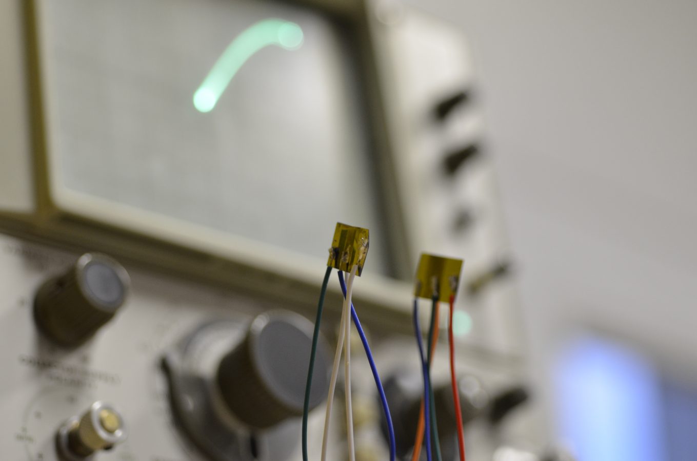
Sam Zeloof is one of this dedicated band, and we've been following his progress for years. While he was still in high school, he turned the family garage into a physics lab and turned out his first simple diodes. Later came a MOSFET, and eventually the Z1, a dual-differential amp chip that is the first IC produced by a hobbyist using photolithography. 

Sam just completed his first year at Carnegie-Mellon, and he's agreed to take some precious summer vacation time to host the Hack Chat. Join us as we learn all about the Z1, find out what improvements he's made to his process, and see what's next for him both at college and in his own lab.

  • Hack Chat Transcript, Part 2

    Lutetium08/14/2019 at 20:05 0 comments

    Sam Zeloof12:43 PM
    In the industry, they use 13.56mhz for all plasma things, a free ISM band. But all the 13mhz equipment is so expensive.

    And about the only thing 10 meters is good for right now, lol

    Sam Zeloof12:44 PM
    Yeah, RIP

    Adam Zeloof12:44 PM
    Give it a few years! (hopefully)

    itsallgoodjames12:44 PM
    @Sam Zeloof what would one expect to spend on a setup like your's

    I don't think the next solar upswing is going to be much to write home about, but maybe.

    Sam Zeloof12:47 PM
    Hard to estimate, I picked up things like a SEM which aren't strictly necessary, but in hindsight you can make basic ICs (probing only or flip chip, no wire bonding) in the low thousands of dollars without stressing too much

    That's pretty approachable. Hmm....

    Sam Zeloof12:48 PM
    @nixie_guy on twitter is doing amazing things, made his own diffusion furnace and a small acrylic vacuum chamber for sputtering copper, all of that costs in the hundreds of dollars

    itsallgoodjames12:48 PM
    @Sam Zeloof how much did you pay for the SEM

    One question: Now that you have access to "real" fab equipment, do you ever find yourself saying, "Man, I wish I had my xxxx instead of this fancy thing"?

    thethoughtemporium12:49 PM
    can confirm. sputtering is cheap. most expensive part by far is the vacuum pump(s). the rest can be done in a mason jar

    Sam Zeloof12:50 PM
    @itsallgoodjames not much, it was thrown out by the university of south carolina and was broken. Look on ebay, the hardest part is transporting them

    Clyde Shaffer joined  the room.12:50 PM

    @thethoughtemporium - No implosions yet? The comments on that article I wrote seemed to think you were doomed for using plain old jars.

    moh.mohx100012:50 PM
    Is it possibly to use standard refrigerator pump for sputtering?

    Sam Zeloof12:51 PM
    @Dan Maloney the "real" fab equipment is so nice and I'm lucky to have the amount of freedom at school that I do, but it is different than working in your own lab for sure. Harder to get away with stupid ideas and missuses of tools!

    thethoughtemporium12:53 PM
    @moh.mohx1000 no. even a decent mechanical pump isn't really that great on it's own. ideally you need a proper 2stage rotary vane pump, and then some secondary pump. diffusion pumps are classic, but im looking into titanium getter pumps as they are buildable in theory

    Sam Zeloof12:53 PM
    @thethoughtemporium you mentioned in your vid that this pump didn't work for sputtering https://www.amazon.com/ZENY-Single-Stage-Economy-Conditioner-Refrigerant/dp/B012CFTYX4/ref=sr_1_4?keywords=vacuum+pump&qid=1565812353&s=gateway&sr=8-4 I actually had the same pump on a small chamber, with nice vacuum fittings and no leaks. Got down below 500mTorr and made nice plasma, probably enough for rough sputtering. I was impressed. But its probably harder without a stainless steel chamber, you need a real vac pump I guess.

    Sam Zeloof12:54 PM
    +1 yeah, real sputtering systems have multiple turbo pumps or crypo pumps to bring the chamber to UHV (nice and clean) before sputtering at ~50 to 100 mTorr

    thethoughtemporium12:54 PM
    things will sputter at 500mtorr but you'll hate your existence the whole time. it's so bloody slow and the coatings are porous as all hell. only time i sputtered that high was when i coated a still damp hornet that took a while to dry under vacuum/plasma

    moh.mohx100012:55 PM
    and a pinning gauge for pressure measuring

    Sam Zeloof12:55 PM
    haha sounds about right. I mainly do thermal evaporation in my chamber, which can be as fast as 100Å/s , orders of magnitude faster than sputtering

    thethoughtemporium12:56 PM
    also, and i found this out the hard way, do not attempt to sputter aluminum/titanium unless you've got a good vacuum system. the oxide layer that builds up prevents material from sputtering. anything else should work fine though. just tried carbon coatings the other day. may have managed diamond...

    Read more »

  • Hack Chat Transcript, Part 1

    Lutetium08/14/2019 at 20:04 0 comments

    OK, let's get started. I'm really excited to have Sam Zeloof here with us today. We've been covering Sam's homebrew ICs for a while now, and it's great to have him for a realtime chat.

    Welcome, Sam! Can you maybe kick things off with a little about yourself?

    Boian Mitov12:00 PM
    Hello everyone :-)

    David大卫 Lanzendörfer12:00 PM
    We're using a laser writer for making the masks

    David大卫 Lanzendörfer12:01 PM
    The funny thing: The guy making the masks has also the English name Sam, but he's Chinese :D

    Sam Zeloof12:01 PM
    Sure! My name is Sam, i'm a second year student in college now and a little over 2 years ago I started acquiring and building the equipment needed to make ICs at home

    philip.lafountain joined  the room.12:01 PM

    Cyrus Tabrizi joined  the room.12:01 PM

    de∫hipu12:02 PM
    "Lanzendörfer" sounds like a very traditional Chinese surname ;-)

    Sam Zeloof12:02 PM
    Last april I succeeded in making a diff amp chip, PMOS, with ~150um gate size and I've been improving things since then to now fab <5um ICs


    https://hackaday.com/2017/02/25/the-fab-lab-next-door-diy-semiconductors/

    HACKADAY DAN MALONEY

    The Fab Lab Next Door: DIY Semiconductors

    You think you've got it going on because you can wire up some eBay modules and make some LEDs blink, or because you designed your own PCB, or maybe even because you're an RF wizard. Then you see that someone is fabricating semiconductors at home, and you realize there's always another mountain to climb.

    Read this on Hackaday

    ICYMI

    David大卫 Lanzendörfer12:03 PM
    I'm not Chinese, I just was looking for a job opportunity to build cool hardware ;-)

    David大卫 Lanzendörfer12:03 PM
    I'm originally from Switzerland

    adam joined  the room.12:03 PM

    Adam Zeloof12:04 PM
    Hi Sam

    Sam Zeloof12:04 PM
    hi adam

    So how did your first year of college go?

    haday12:05 PM
    I'm not familiar with your project, but I'm guessing you are working with Si substrate. Where are you sourcing it?

    thethoughtemporium12:06 PM
    hi sam, biggest question where do you get your photoresist?

    Sam Zeloof12:06 PM
    Pretty well, lots of work overall but I had some great experiences and was lucky enough to start working on other stuff right away. Outside of classes, I am working in the nanofab there and have started my own lab in that department to develop new fab tools and processes. Not much info on that yet but hopefully soon I can talk more about it, make a website, etc

    Sam Zeloof12:07 PM
    Yup, Si substrate. you can get small quantities on ebay or here https://www.universitywafer.com/

    David大卫 Lanzendörfer12:08 PM
    Sam: Our lambda is 500nm at the moment

    David大卫 Lanzendörfer12:08 PM
    January we'll get access to an actual fab with a lambda of 250nm!!

    ammater77 joined  the room.12:09 PM

    Sam Zeloof12:09 PM
    thethoughtemporium ! I saw one of your recent youtube vids and was going to reach out and offer you some photoresist, but couldn't find a contact button on your YT page. In the beginning I used PCB resist from Aliexpress (i think) but if you live in the US most companies will give out samples of their resists. Other than that, make friends in the industry...

    David大卫 Lanzendörfer12:09 PM
    The entire PDK and process flow will be published online

    itsallgoodjames12:09 PM
    am i able to purchase one of your homemade ic's

    haday12:09 PM
    I'm guessing you are working with already doped wafers?

    David大卫 Lanzendörfer12:10 PM
    Yeah, at the moment 4 inch, pdoped, single side polished, prime wafers, but the process is designed

    Sam Zeloof12:10 PM
    haday, yup. Commonly for NMOS circuits you start with a p-type bulk doped wafer, and the opposite is true for PMOS. For CMOS, you can start with either but commonly p doped are used, then to make P channel devices you implant a N-type well

    David大卫...

    Read more »

View all 2 event logs

Enjoy this event?

Share

Discussions

Victoria Suarez wrote 12/05/2019 at 10:47 point

The best site! https://hackaday.io/

  Are you sure? yes | no

Interested in attending?

Become a member to follow this event or host your own