 Lutetium
 Well crap that didnt work
 I blame Google
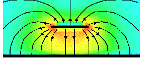
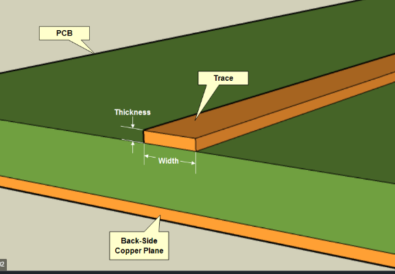
So these images show a trace above a ground plane and the field around it.
![]() Got it, thanks
Got it, thanks
 strawberry fields forever?
So when we DONT match the impedance a reflection occurs. Truth be told we live with tehse reflections all over the place but...
Enter the series resistor, I used to put 22 Ohm resistors in series to absorb the signal that got away from me and is bouncing up and down the trace
are termination resistors fitting into this picture too or no?
A reflection occurs when the receiver doesn't absorb 100% of the signal
if the transmitter is 50Ohms and the receiver is 55 ohms than a percentage will be reflected.
If the transmitter doesn't absorb it it will be reflected again
Is that kinda clear or should I talk more about absobing the reflection when they ARENT matched?
By the way, my CAD package calculates the trace width for me
which?
(CAD package)
Altium, Labcenter
Eagle might, Ted you still there?
Labcenter makes Proteus. Kicad also will with the right addon
![]() So from my understanding by adding a serial R on the tx side we allow the signal to reflect from unmatched receiver and to be absorbed at the receiver side. And that does not influence the reception quality because the receiver does not "see" the reflection caused by itself?
So from my understanding by adding a serial R on the tx side we allow the signal to reflect from unmatched receiver and to be absorbed at the receiver side. And that does not influence the reception quality because the receiver does not "see" the reflection caused by itself?
Yes. AND its not radiated as much and it doesn't keep bouncing around creating noise, including FCC emmision noise
![]() right
right
I think using firehose to fill a small cup vs. using garden hose vs. using garden hose with restrictor attachment
is that right direction? "spilled water" in my analogy would be reflected signal
I am trying to get images off my CAD station but the image upload problem is making it tough
Think of a trough of water.
![]() But the restrictor is on the tap and the cup is a closed system
But the restrictor is on the tap and the cup is a closed system
and a wave
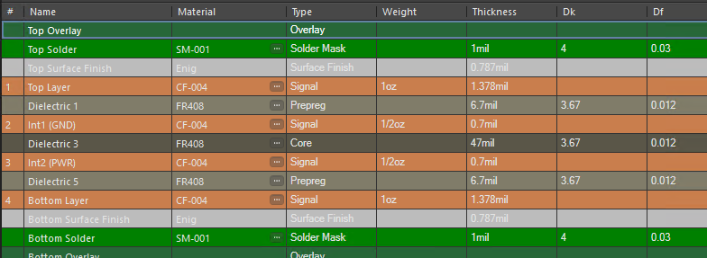
Cheap PCB material has a more variable Dielectric constant and more absorption in general usually. Oshpark has a good hi freq material (FR408) for their 4 layer boards and JLBPCB has some Rogers materials available (I use 2313)
Flex pcb material polyamide also has good hifreq properties.
Also before I forget there are great calculators for some of this online. So if I move into wave length these here may help: https://www.microwaves101.com
https://www.everythingrf.com/rf-calculators
As frequencies go up, the distance represented by a wavelength goes down.
Everyone understand what I mean by wavelenth? Basically Planks constant and why those little holes in yoru microwave oven door let light out but keep microwaves in
250 mhz has a wavelength of 47”, 500 mhz has a wavelength of 23”
Sounds huge right!
When a trace gets to be 1/4th of a wavelength we really DO need to start using atransmission line
(transmission line = stripline = trave over ground plane)
So if we have 500mhz component, anything near 6”/150mm or greater needs to be done as transmission line known as a microstrip and others like stripline, waveguide, etc
so think 500Mhz and 6" , at 500 mhz RADIAN Freq or rise time
the trace officially becomes an RF antenna at 6"
so with a 100mhz PCIe it's pretty much everything needs to be a transmission line?
Here is a radar I am working and will be in a future video
 Awesome free calculators: AppCAD (available free by Avago web site). QUCS (open source simulator, has awesome and very accurate T-line solver in it) qucs.sourceforge.net
Whats the risetime of the signal though?
mmm
PCIE Gen 4 is a tough nut, all is doen as controlled impedance
QUOCs rocks.
Hi Ben!
Hey Bil!!
NICE
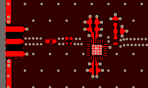
looks like you made a PCB coax almost?
So here is a trace coming in on the left, there is an SMA connector soldered there and the cone tries to smoothly transition the signal from the connector to the PCB
YES! We are making coaxes out of PCBs
what kind of frequency is this designed for?
So the vias right along the trace are "shielding" vias but also stitch the return path in the inner layer to the shield on the top layer
2.54ghz and higher
![]() It starts getting iffy when half wavelength equals the via period.
It starts getting iffy when half wavelength equals the via period.
We use the smallest parts we can typically, there are tricks like flipping teh inductor over and soldering them upside down to make the path and inductance shorter
Yup. So notice all of the other vias, (this is about an x2 or x3 view bytw)
btw
at 1/20th of a wavelenth the shield can start to "stand", little resonances build up
Think of a sheet blowing in the wind. and then start tacking it down every few inches, same concept
I am out of time and don't think I explained this very well, (don't ever tear a finger off, it screws with your typing)
Good timing, Bil...
So I hate to break up the party, but we're coming to the one-hour mark and we need to let Bil get back to work if he needs to. Feel free to stick around and keep the chat going, though, if time allows. For now, I'll just say thanks to Bil for stepping up on short notice, and for the great chat - I learned a lot.
thanks for explaining what you did. Much appreciated.
Did anybody get something they didn't previously know?
![]() Thanks Bill
Thanks Bill
Absolutely!
 Yeah, this was great!
I recommend the video I referenced above as I talk faster than I type
which video?
![]() Thanks for this, i get it a lot more, but still have a way to go
Thanks for this, i get it a lot more, but still have a way to go
@Dan Maloney The image paste thing seems to be a mode it gets into with a keystroke, I just don't know which keys
![]() Yes, thanks. Your video/blogs have been very informative, too. Look forward to more.
Yes, thanks. Your video/blogs have been very informative, too. Look forward to more.
I'll be posting a transcript with links in a few minutes
The pics were great
 Yeah, thanks!
Yeah, I'm going to experiment with that for future chats. Sorry for the trouble
https://www.youtube.com/watch?v=STCGzanAyR0
Thanks to everyone for coming. Don't forget that next week we'll be talking about Alternative Photography with Pierre-Loup Martin
https://hackaday.io/event/166697-alternative-photography-hack-chat

Alternative Photography Hack Chat
Pierre-Loup Martin joins us for the Hack Chat on Wednesday, October 2, 2019 at noon PDT. Time zones got you down? Here's a handy time converter! It seems like the physics of silicon long ago replaced the chemistry of silver as the primary means of creating photographs, to the point where few of us even have film cameras anymore, and home darkrooms are a relic of the deep past.
you rock Bil!
Ask Ben if he wrote that part of the app. ;)
![]()
https://hackaday.com/2018/09/28/inductance-in-pcb-layout-the-good-the-bad-and-the-fugly/

Inductance In PCB Layout: The Good, The Bad, And The Fugly
When current flows through a conductor it becomes an inductor, when there is an inductor there is an electromagnetic field (EM). This can cause a variety of issues during PCB layout if you don't plan properly, and sometimes we get burned even when we think we have planned for unwanted inductance and the effects that come with them.
thanks @Bil Herd , I didn't understand before your chat why the trace width is important for the impedance, but makes sense now, being a capacitor
Discussions
Become a Hackaday.io Member
Create an account to leave a comment. Already have an account? Log In.