 Dan Maloney
@Christoph Post 'em. We'll try to get to them if we see them.
 @Christoph Or I mean, ask now.
I'm doing some other work but I have the chat window open.
Hi @Elijah
I think we're overachievers.
 Im always early, i usually have some type of log-in issue. But it looks like im ok today!
Woohoo! Only because you logged in early.
Exactly!
 My question would be: what should an ENIG finish look like to be considered acceptable? I've had two boards with different ENIG quality - one soldered fine, the other failed. "ok" should be somewhere in between. I have pictures, too
I believe that ENIG is covered under IPC-4552
That's the standard that says what's acceptable and what's not.
The problem is two-fold.
One, it's not all that wettable -- which means that the solder tends to ball up rather than spread out over the surface.
Secondly, if the coating is too thick, the intermetallics might not form, which relates to wettability, but also to reliability.
Even if it wets, without intermetallic formation at the interfacial layers, your parts will start to fall off the board during thermal cycling.
Upload the photos and we'll take a look.
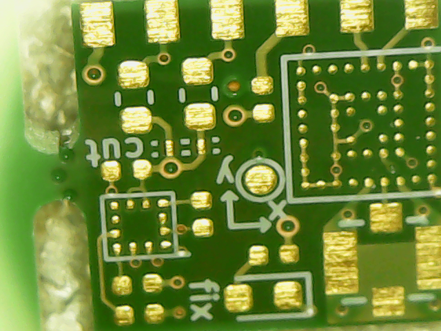
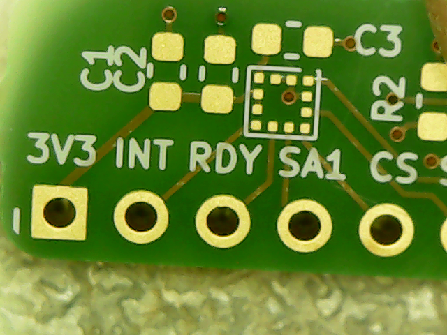
Can you show me a less blurry image of number 1?
Also -- do you have pictures of these boards with soldered components on them?
I'll try - the thing is the kids aren't in bed yet and tend to cause some trouble when I get out the good stuff
Ah.
Well I'll just riff a little until then.
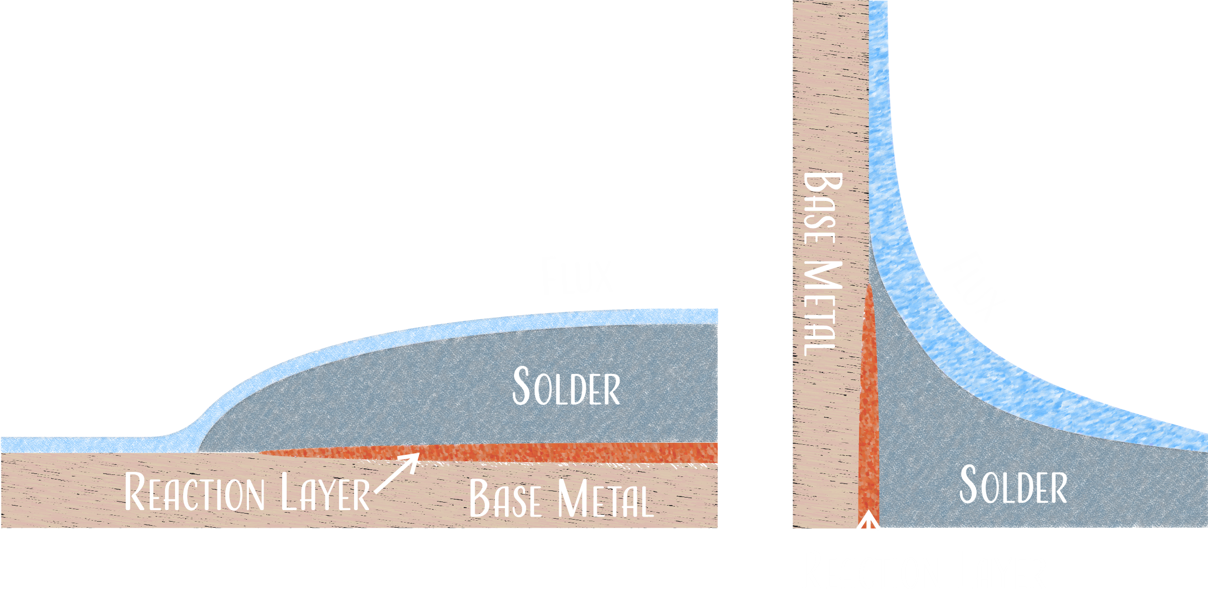
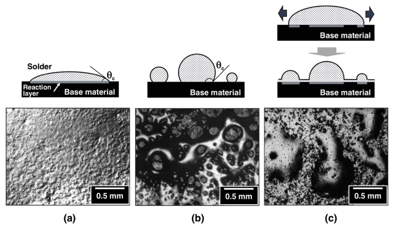
When solder-paste is heated, the first thing that melts is the flux. It spreads out over the surface in a process called "wetting"
Wetting is determined by the adhesive and cohesive forces between a liquid and its surroundings.
The surface roughness comes into play too.
Anyways -- the first thing that melts is the flux.
It spreads out over a surface and chemically de-oxidizes is.
does the dispensed paste blob get flatter as the flux melts or will it stay in shape?
Then at a slightly higher temperature, the solder metal melts and begins to flow over the surface.
(actually I can answer that myself by recalling what I see when I solder on a hot plate - it gets flatter)
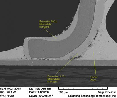
 It's also bad if the solder dissolves enough of the gold so that the joint then comes into physical contact with the nickel layer. This cannot happen during normal reflow process, but can be done during manual soldering...
The "blob" will move along metal surfaces until it is stopped by Solder-Resist.
So, as the solder becomes liquid, it begins to react with the other metals present. Let me see if I can grab a picture.
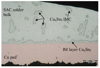
At the reaction layer -- Intermetallics form -- these are essentially metal crystals that behave like pure metals.
If the intermetallic layers get too thick (pictured above) or large crystals form in the bulk of the solder, the solder joint can fail over time.
Now you said that the boards didn't solder well.
That could be a fabrication issue, that could be an assembly issue.
one did solder well - the one with the smoother finish
From what I saw in the first picture you sent me sure does look like a fabrication issue.
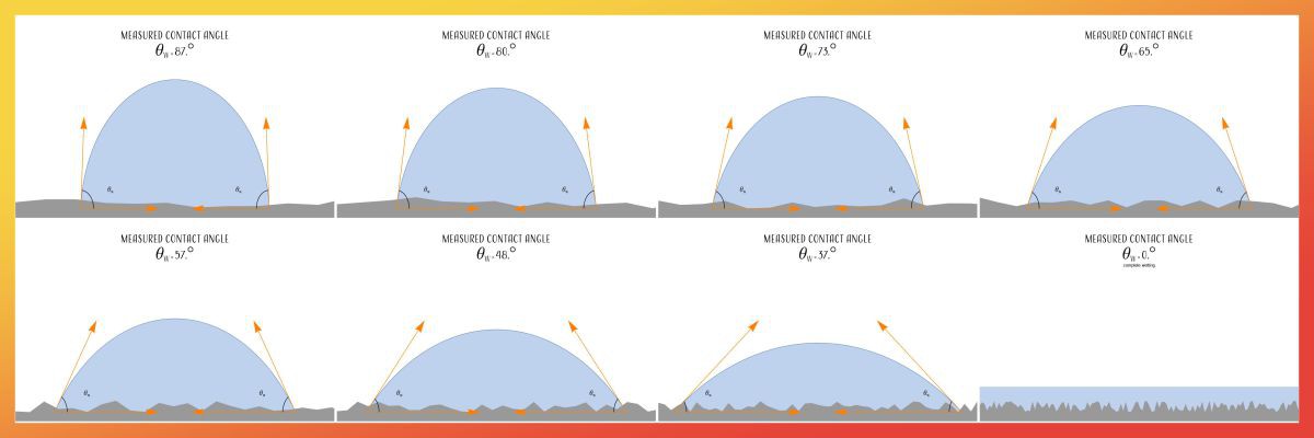
The surface roughness appeared to be crazy-rough. Which means the solder cannot properly spread over the surface in a process called "wetting".
The crystal size does affect solderability and is the reason why hard gold is so difficult to solder...
I wanted to see a clearer image before I went down this route.
But if the surface is too smooth, the solder will tend to ball up, or non-wet.
I might be able to throw a better picture into chat later - we'll see
So a tiny bit of roughness (like on the micron scale) is good.
But when you have large undulations like what appears in that picture, all bets are off.
Solder pads are meant to be largely planar shapes.
undulations on the 10^-4 & 10^-5 range are a fabrication mess up.
the pads also seemed to be slightly "spherical" which is also visible on the first picture
@Elijah take a look at @Christoph 's first picture he shared.
Elijah has more fab experience than I do. I'm a bit curious as to what caused the striations. It seems like the mistake happened at the electroless nickel deposition step.
But there's a chance it happened when they sanded the board, before they ever put the nickel down.
And that's what I'm guessing. But I'll take @Elijah word over mine.
He might not be on at the moment -- we're not scheduled for another few minutes.
yut, half an hour to go nd I kinda feel bad for starting the discussion early
Okay -- I'm going to go out on a limb and say it happened after the copper plating and before the electroless nickel.
The copper should be chemically cleaned -- but some processors put the panels through a "scrub-brush" process first. Basically a conveyor with a spinning wheel above it.
If I had to guess -- and this is a big guess, with lots of assumptions.
Whatever board went through before yours was thinner -- and they forgot to readjust the height of the machine before board one went through.
So it "scrubbed" too hard.
Then they applied the electroless nickel
And then the gold.
The board should never have made it through QC.
Should never have even had the gold applied.
@Elijah if you're there buddy, jump in. I'm just making things up at this point.
Essentially though -- if you ever see a surface finish that is that bad -- you should be able to RMA the boards back to your supplier.
Hey Mark, sorry! let me read whats going on. I was getting a few things finished before we start
No worries -- @Christoph has a ENIG board with bad surface finish -- see his post a few pages above. Look at the first picture.
What do you think happened?
And feel free to disagree with me. I was making huge leaps of the imagination.
if you can't scroll up that far I can PM the picture to one of you
I was about to tell him his interlocking framastan joint failed.
@Christoph its a little hard to tell. We would have to cross-section the board to give a solid answer. But from the naked eye, the deep parallel grooves make me think that the copper was scrubbed far too aggressive before the gold was added
And you are right on with that causing the solderability issues @Mark J Hughes
sounds pausible
@Elijah Whew! I guessed that too! Well, even blind squirrels find nuts and all that.
@Christoph take that picture and go back to your fabrication and complain.
Do you mind sharing who you used?
@Christoph were both board manufactured at the same shop?
that was aisler (or rather the board house they use). happened only once and I later received good boards again
they haven#t commented on that one bad case though
They might have more than one board shop they partner with.
and yes, Mark is right. That quality is unacceptable.
thank you very much! I have to leave for a while but I'll surely get back later
Yeah they usually use multiple board shops. I am not familiar with Aisler but many brokers often use a "get what you pay for" price point. If you paid a fair price, definitely get a remake!
 So, quite a bit of "preamble" discussion here, which is great. I'll try to capture all of it for the transcript, which I'll post publically after the chat. We'll get started with the "official" chat in about 10 minutes.
And welcome Elijah and Mark!
Hey @Dan Maloney thanks for having us!
Thanks @Dan Maloney -- hey would it be appropriate to promote our PCB design course? Or is this not the forum for that?
![]() What is the topic tonight?
What is the topic tonight?
https://hackaday.io/event/169956-pcb-finishes-hack-chat

PCB Finishes Hack Chat
Mark Hughes and Elijah Gracia will host the Hack Chat on Wednesday, March 11, 2020 at noon Pacific Time. Time zones got you down? Here's a handy time converter! Once those traces are formed, however, there's more work to be done.
@Mark J Hughes - I think it's OK to mention that. It seems like this would be a group that might want to know about that

If anyone is interested in learning the basics of Rigid PCB layout, we're starting a course at the end of the month.
If it goes well, we will extend it to Rigid-Flex design.
And we're paying for 50 people's projects to be built (fabbed, assembled, parts & shipping)
![]() any cost for the course?
any cost for the course?
100% free
I mean, we kinda expect you to name your first-born "Elijah"
But we haven't found a lawyer willing to draw up the contracts yet.
Its the least you could do!
No -- the least they could do is name their first-born "Mark".
I mean -- that's easily 2 fewer letters.
![]() Sorry, he's already named and the paperwork would a pain to change it.
Sorry, he's already named and the paperwork would a pain to change it.
Hello everyone, welcome to the Hack Chat! Today we've got Mark Hughes and Elijah Gracia from Royal Circuit Solutions to talk to us about PCB finishes.
Discussions
Become a Hackaday.io Member
Create an account to leave a comment. Already have an account? Log In.