Close
0%
0%

SkyWater PDK Hack Chat

Absolutely fabless

Wednesday, September 16, 2020 12:00 pm PDT Local time zone:
Hack Chat
Similar projects worth following

Tim "mithro" Ansell, Mohamed Kassem, and Michael Gielda will host the SkyWater PDK Hack Chat on Wednesday, September 16, 2020 at noon Pacific Time.

Time zones got you down? Here's a handy time converter!

Join Hack ChatWe've seen incredible strides made in the last decade or so towards democratizing manufacturing. Things that it once took huge, vertically integrated industries with immense factories at their disposal are now commonly done on desktop CNC machines and 3D printers. Open-source software has harnessed the brainpower of millions of developers into tools that rival what industry uses, and oftentimes exceeds them. Using these tools and combining them with things like on-demand PCB production and contract assembly services, and you can easily turn yourself into a legit manufacturer.

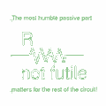
This model of pushing manufacturing closer to the Regular Joe and Josephine only goes so far, though. Your designs have pretty much been restricted to chips made by one or the other big manufacturers, which means pretty much anyone else could come up with the same thing. That's all changing now thanks to SkyWater PDK, the first manufacturable, open-source process-design kit. With the tools in the PDK, anyone can design a chip for the SkyWater foundry's 130-nm process.  And the best part? It's free -- as in beer. That's right, you can get an open-source chip built for nothing during chip manufacturing runs that start as early as this November and go through 2021. 

We're sure this news will stir a bunch of questions, so Tim Ansell, a software engineer at Google who goes by the handle "mithro" will drop by the Hack Chat to discuss the particulars. He'll be joined by Mohamed Kassem, CTO and co-founder of efabless.com, and Michael Gielda, VP of Business Development at Antmicro. Together they'll field your questions about this exciting development, and they'll walk us through just what it takes to turn your vision into silicon.

  • Hack Chat Transcript, Part 2

    Dan Maloney09/16/2020 at 20:17 0 comments


    Tim Ansell12:44 PM
    @Troy Benjegerdes My general thinking is that if 130nm is successful I will be able to convince foundries to open source more advanced nodes where a Linux class processor is a *lot* more interesting.

    Mohamed Kassem12:44 PM
    "steve" what's your @ ID can't find you?

    Nathan Kohagen12:45 PM
    The Skywater fab in Minnesota was the main Cypress Semiconductor fab. The PSoC3 (8051) and PSoC5 (ARM Cortex M3) family of chips (which I was one of the designers of) were on this 130nm process. And regarding the cryo question earlier in this chat, to my knowledge this 130nm process has not been characterized down to cryo temps. It is public knowledge that the DWave (quantum computing) superconducting (cryo) chips were fabbed at the Cypress Minnesota fab a decade ago so the fab is capable of more exotic fab process recipes. Another note: the Skywater fab is a secure fab (has information control policies) that allows it to be used for chips that are strategically important to US national security. That fab is a very important fab to the future of the US semiconductor industry.

    Troy Benjegerdes12:45 PM
    @Tim Ansell you are probably right, unless I can build a single wafer that boots linux with 8TB of 3-d non-volatile ram ;)

    steve12:46 PM
    @steveulti

    Mohamed Kassem12:46 PM
    @Nathan Kohagen I second that ..

    Tim Ansell12:46 PM
    The great thing about open source, and something I want to promote, you don't have to ask for permission - you can just go do things I'm not directly interested in without needing to chat with me.

    Troy Benjegerdes12:46 PM
    @Art Scott you mention Posit.. my first job in College was working for John Gustafson

    Mohamed Kassem12:46 PM
    -----------------------

    Full Open Source RTL2GDS Compiler

    https://github.com/efabless/openlane

    Open Source Manufacturable 130nm PDK

    https://github.com/google/skywater-pdk

    ----------------------------

    Tim Ansell12:47 PM
    My goal is to build a thriving ecosystem of people doing everything from pretty "boring" things to crazy stuff like the adiabatic circuits that @Art Scott is super interested in.

    Patrick Van Oosterwijck12:48 PM
    Much more interesting than another Linux bootable micro which you can have for $5 nowadays...

    Mohamed Kassem12:48 PM
    @Steve very soon

    Tim Ansell12:49 PM
    Someone asked earlier about documentation on the analog side of things

    Troy Benjegerdes12:49 PM
    so who can help me write a Posit unit for rocket-chip

    Mohamed Kassem12:49 PM
    @Steve we are finishing the IO's so we can push several chips including Caravel

    Troy Benjegerdes12:49 PM
    (or vhdl to plug into leon-sparc or noel-RiscV from Gaisler's GRLIB)

    Tim Ansell12:49 PM
    I have a "work in progress" pull request for the repo at https://github.com/google/skywater-pdk/pull/136 which adds a lot of detail about the various supported devices

    Steve Kelly12:49 PM
    @Mohamed Kassem is the base SoC for the initial shuttle decided?

    Patrick Van Oosterwijck12:50 PM
    @Tim Ansell thanks for the link to that PR

    Mohamed Kassem12:50 PM
    @Steve Kelly call it 75>#/span###

    W5VO12:50 PM
    Does this process variant support some of the BCD / analog devices that Skywater offers?

    W5VO12:51 PM
    oh, just saw that.

    Tim Ansell12:51 PM
    The devices included are;

    Bipolar (NPN)

    Bipolar (PNP)

    MiM Capacitor

    Vertical Parallel Plate (VPP) capacitors

    SONOS cells

    SRAM cells

    Diodes

    11V/16V NMOS FET

    1.8V NMOS FET

    1.8V low-VT NMOS FET

    20V NMOS FET

    20V isolated NMOS FET

    20V native NMOS FET

    20V NMOS zero-VT FET

    3.0V and 5.0V native NMOS FET

    5.0V/10.5V NMOS FET

    NMOS ESD FET

    10V/16V PMOS FET

    1.8V PMOS FET

    1.8V high-VT PMOS FET

    1.8V low-VT PMOS FET

    20V PMOS FET

    5.0V/10.5V PMOS FET

    Generic Resistors

    P- poly precision resistors

    P+ poly precision resistors

    Varactors

    Tim Ansell12:52 PM
    I want to get the PR merged ASAP but it still needs some finishing touches.

    Art Scott12:52 PM
    @Troy Benjegerdes posithub PACoGen

    PACoGen: Posit Arithmetic Core Generator .... verilog file ... lets do it

    Sam Ellicott joined the room.12:53...

    Read more »

  • Hack Chat Transcript, Part 1

    Dan Maloney09/16/2020 at 20:15 0 comments

    OK, welcome to the Hack CHat. Had some trouble there for a bit, but we're good now. I'm Dan, I'll be moderating today. Let's welcome Tim Ansell to the chat to talk about SkyWater PDK

    Michael Gielda12:01 PM
    Hi! Testing :)

    Oh right - and Michael Gielda, and hopefully Mohamed Kassem soon. Welcome!

    Mohamed Kassem joined the room.12:02 PM

    Can Tim and Michael start us off with a little intro? And Mohamed now - gang's all here. Welcome!

    Tim Ansell12:03 PM
    Hello everyone!

    Michael Gielda12:03 PM
    Tim should do the honors! He's the reason we're here.

    Mohamed Kassem12:04 PM
    Hi Everyone! I was in the other channel!

    steve joined the room.12:04 PM

    Tim Ansell12:04 PM
    So, we are here to chat about the "skywater-pdk" which was recently released by Google

    Tim Ansell12:04 PM
    It can be found at https://github.com/google/skywater-pdk

    Tim Ansell12:05 PM
    A PDK is an extremely important part required to create an integrated circuit like a CPU or similar.

    Yann Guidon / YGDES12:05 PM
    Welcome Mohamed !

    Tim Ansell12:06 PM
    The skywater-pdk currently contains the low level information needed to create a manufacturable IC on SkyWater Foundry's SKY130 process -- which is roughly a 130nm process technology.

    kira joined the room.12:06 PM

    Tim Ansell12:07 PM
    There is lots of documentation about the contents of the PDK found at https://skywater-pdk.readthedocs.io/en/latest/ -- I push a pretty big drop of new information yesterday that I have yet to announce.

    Tim Ansell12:07 PM
    The PDK contains things like the data needed for simulating the transistors and standard cells.

    What would the 130-nm process represent historically? Like, how long ago was 130-nm cutting edge tech?

    Tim Ansell12:08 PM
    130nm is about a ~20 year old technology.

    Mohamed Kassem12:08 PM
    2003'ish

    Tim Ansell12:08 PM
    I believe "high performance" CPUs created with 130nm technology were just hitting the market in 1999

    Michael Gielda12:08 PM
    So it's still 21st century tech! that used to mean it's new ;)

    Tim Ansell12:09 PM
    I actually have a "living document" at https://j.mp/si130nm which is suppose to include a bunch of information around what is possible with 130nm

    THere were still a lot of interesting chips 20 years ago though, right>

    !This message failed to send, please try again.

    Art Scott12:09 PM
    130 less leaky ... a good thing

    Jarrett12:09 PM
    oh wow

    Jarrett12:10 PM
    I like inspirational information, having no frame of reference for what can be done with the given area

    Tim Ansell12:10 PM
    The Intel PentiumB 4 Processor, Intel Itanium2 Processor and IBM PowerPC 970 all done on 130nm process nodes

    Tim Ansell12:10 PM
    These days 130nm is generally used for microcontrollers

    Yann Guidon / YGDES12:10 PM
    130nm is a sweet spot for prices, speed, power and a mature process has much fewer unknowns

    keyes118 joined the room.12:11 PM

    Patrick Van Oosterwijck12:11 PM
    How's the process for analog / power / HV?

    Tim Ansell12:11 PM
    As @Yann Guidon / YGDES points out 130nm is just before you start seeing a lot of more complex physics needing to be involved in modeling the process

    Mohamed Kassem12:11 PM
    I think we should all look at the fact that this is the first manufacturable open source PDK. There are "many" applications that benefit from the quality of components and the price/cost

    Tim Ansell12:12 PM
    I should also mentioned I'm not an ASIC / IC designer, I'm a software engineer at heart. @Mohamed Kassem is the person who can answer more technical questions around that.

    Mohamed Kassem12:12 PM
    @Patrick Van Oosterwijck it has a good array of devices to support unto 20V (need to confirm if there is more)

    So the process limit is more a practical limit that something imposed arbitrarily for like IP reasons or something?

    Tim Ansell12:13 PM
    I *believe* 130nm is a node that a lot of analog designers like because of the physics.

    dbellix12:13 PM
    Indeed it is not the last, but I think that for many small companies and universities it is a valuable approach for testing ideas, especially...

    Read more »

View all 2 event logs

Enjoy this event?

Share

Discussions

Interested in attending?

Become a member to follow this event or host your own