Close
0%
0%

Heavy Copper PCB Hack Chat

Big, fat, beautiful traces

Wednesday, November 10, 2021 12:00 pm PST Local time zone:
Hack Chat
Similar projects worth following

Mark Hughes and Greg Ziraldo will host the Hack Chat on Wednesday, November 10 at noon Pacific.

Time zones got you down? Try our handy time zone converter.

Join

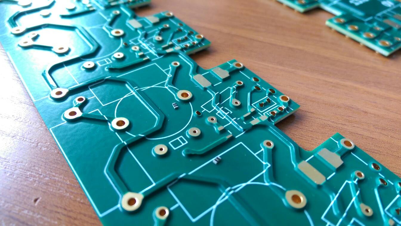
For as useful as printed circuit boards are, they do seem a little flimsy at times. With nothing but a thin layer -- or six -- of metal on the board, and ultra-fine traces that have to fit between a dense forest of pads and vias, the current carrying capacity of the copper on most PCBs is somewhat limited. That's OK in most cases, especially where logic-level and small-signal currents are concerned. But what happens when you really need to turn up the juice on a PCB?

Enter the world of heavy-copper PCBs, where the copper is sometimes as thick as the board substrate itself. Traces that are as physically chunky as these come with all sorts of challenges, from thermal and electrical considerations to potential manufacturing problems. To help us sort through all these issues, Mark and Greg will stop by the Hack Chat. They both work at quick-turn PCB assembly company Advanced Assembly, Mark as Research Director and Greg as Senior Director of Operations. They know the ins and outs of heavy-copper PCB designs, and they'll share the wealth with us.

  • Hack Chat Transcript, Part 3

    Dan Maloney11/10/2021 at 21:08 0 comments


    Mark J Hughes1:02 PM
    I'll put you in touch with my buddy in Cad/Cam and he'll tell you how to accomplish your goals affordably!

    Greg Ziraldo1:02 PM
    I suppose so. ;) This has been fun guys!

    Mark J Hughes1:02 PM
    Thanks @Dan Maloney

    Dave Blundell1:02 PM
    thank you... sorry I missed most of it, had to pick up daughter

    Dan Maloney1:02 PM
    You bet, thanks to you both and to everyone for the great chat!

    Mark J Hughes1:02 PM
    No worries man. We do free engineering services for peeps.

    Dan Maloney1:03 PM
    I'll be posting a transcript shortly. @Dave Blundell

    Greg Ziraldo1:03 PM
    Feel free to reach out to me directly at gziraldo@aapcb.com with questions as well.

    Mark J Hughes1:03 PM
    Oh -- it was epic Dan -- probably the best hack chat ever. Wanna know why?

    Mark J Hughes1:03 PM
    GREG-FREAKING-ZIRALDO!

    Mark J Hughes1:03 PM
    Hip-hip!

    Mark J Hughes1:03 PM
    Hooray!

    Mark J Hughes1:03 PM
    Hip-hip!

    Mark J Hughes1:03 PM
    Hooray!

    Dan Maloney1:03 PM
    I saw that coming...

    Mark J Hughes1:03 PM
    Hip-hip!

    Mark J Hughes1:03 PM
    Hooray!

    Greg Ziraldo1:03 PM
    Good lord. :|

    Nicolas Tremblay1:03 PM
    next time, we only invite Greg

    Mark J Hughes1:04 PM
    Ouch Nicolas -- that hurt me right in the feels.

    Mark J Hughes1:04 PM
    ;)

    Greg Ziraldo1:04 PM
    Ha! Cheers all, let's do this again!

    Dan Maloney1:04 PM
    Cool stuff, thanks so much! We'll be taking a couple of weeks off to do Remoticon and Thanksgiving, so tune in again in December when we pick it back up. Thanks all!

  • Hack Chat Transcript, Part 2

    Dan Maloney11/10/2021 at 21:07 0 comments


    Greg Ziraldo12:28 PM
    @Jason - stick to one weight. The minimal value-add to your design will be drastically over shadowed by the high manufacturing cost.

    Mark J Hughes12:28 PM
    3) How much current you'll put through the trace

    Mark J Hughes12:28 PM
    And then you can get a great first-order estimate for your trace-width.

    alexwhittemore12:29 PM
    @Greg Ziraldo but selective copper thickness is a thing and possible?

    Mark J Hughes12:29 PM
    The best part is that these equations all assume a single trace with no ground plane sucking heat away. So these are all high-end estimates.

    Mark J Hughes12:30 PM
    @Dan Maloney What are the filesize limits on here?

    Jason12:30 PM
    @Greg Ziraldo - perfect thanks for the advice

    Greg Ziraldo12:30 PM
    Sure. Same as selective soft/hard gold plating. You would use photo resist as a mask to "build up" areas. Again...this pushes the envelope of manufacturability and more into the "arts and crafts" world.

    Kearney Lackas12:30 PM
    I think this might be the same as another question but...is it easier to do select thick layers or more layers (acting in parallel). Say a 6 layer x 1 oz board using 3 layers in parallel for a particular trace or a 4 layer board with 3oz copper on top/bottom. And is there a transition point... For example, is the trade between 3x 2oz layers vs 1x 6oz layer the same?

    Dan Maloney12:30 PM
    I'm not sure, actually. Don't think we've ever run up against a limit before.

    Mark J Hughes12:30 PM
    See Greg -- they're all pinging you man. I stand in the shadow of your greatness once again.

    Dan Maloney12:30 PM
    Give it a shot and we'll see

    Mark J Hughes12:31 PM
    Perhaps once, the winds will blow and you'll sway, and I shall grab a glimpse of the light that shines around you.

    Greg Ziraldo12:31 PM
    Whatever Mark. ;)

    Mark J Hughes12:31 PM

    AdvancedAssembly_HeavyCopperCalculations_001-100C_WonB.zip
    9 MB

    Download File

    Dan Maloney12:32 PM
    So somewhere north of 9MB, I guess ;-)

    Mark J Hughes12:32 PM
    Okay -- I just uploaded a file Greg and I created programmatically for a variety of copper weights, temp increases and what not. Enjoy!

    Mark J Hughes12:33 PM
    @Kearney Lackas That brings up a good point. If you don't have room to run the copper all on one layer, you can split it across multiple layers. It is very important that you keep your stackup balanced symmetrically around the mid-plane

    Mark J Hughes12:33 PM
    Otherwise the part will turn into a potato chip during reflow.

    Mark J Hughes12:34 PM
    Here's something else to consider. Good luck doing rework on a heavy copper trace.

    Greg Ziraldo12:34 PM
    @Kearney Lackas additionally the lower your copper weight it, the easier to etch, the easier to fabricate, ultimately giving you far better yields, repeatability and of course cost.

    Mark J Hughes12:35 PM
    Copper absorbs heat better than any metal other than silver.

    bboyes12:35 PM
    Nice file thanks. Do you have a good reference to available PC bus bars? Rogers (maybe) used to make some. I haven't looked in years.

    Mark J Hughes12:35 PM
    I tend to reference Douglas Brooke's a lot for this sort of thing.

    Jason12:35 PM
    @Mark J Hughes - +75C max ambient and +5C temp rise (guesstimate), 25A max steady state, 75A peak for 1s.

    Mark J Hughes12:35 PM
    He's got a lot of free articles on his website -- I haven't looked to see if bus-bars are free lately.

    Mark J Hughes12:35 PM
    But I'm sure he's got them in his textbook.

    Greg Ziraldo12:36 PM
    Great point Mark. We have been talking PCB, we have not even started talking about populating high Cu PCBAs! *custom reflow profiles have entered the chat*

    Mark J Hughes12:36 PM
    Here's his textbook.

    Mark J Hughes12:36 PM

    https://amzn.to/3qvZ7mV

    AMAZON

    PCB Design Guide to Via and Trace Currents and Temperatures

    PCB Design Guide to Via and Trace Currents and Temperatures [Douglas Brooks, Johannes Adam] on Amazon.com. *FREE* shipping on qualifying offers. PCB Design Guide to Via and Trace Currents and Temperatures

    Read this on Amazon

    Mark J Hughes12:36 PM
    @Jason -- what's...

    Read more »

  • Hack Chat Transcript, Part 1

    Dan Maloney11/10/2021 at 21:06 0 comments

    Dan Maloney12:00 PM
    OK, everyone, let's get started. I'm Dan and I'll be the moderator today along with Dusan for Mark Hughes and Greg Ziraldo. They're both from Advanced Assembly and they're here today to talk about big copper. Welcome!

    Mark J Hughes12:00 PM
    Hi everyone! I'm Mark

    Brian Lindahl12:01 PM
    Hi, Mark...

    Mark J Hughes12:01 PM
    I work with Greg at Advanced Assembly in beautiful Auroroa, Colorado. We are the original quick-turn industry experts, and we make boards as fast as you need them -- including in a single shift.

    Dan Maloney12:02 PM
    So maybe we can start with a little about your backgrounds?

    Dan Maloney12:02 PM
    I type too slow ;-)

    Mark J Hughes12:02 PM
    We're so big, we have our own pick teams at the major parts distributors -- so your parts are likely going to show up the same morning that your parts are.

    Mark J Hughes12:02 PM
    We can stuff 'em and get 'em back on the plane back out to you.

    Mark J Hughes12:02 PM
    We're here to answer anything you want to know about Heavy Copper (generally regarded as 1.5 oz or greater)

    Mark J Hughes12:03 PM
    And we can help you solve any other PCB and PCBA problems you might have.

    Greg Ziraldo12:03 PM
    Glad to be here Dan! Hi everyone, I'm Greg. I am over Operations (engineering, manufacturing and supply chain) at Advanced Assembly. I have been with AA for a little over 4 years and I have been in the high-reliability side of EMS for nearly 18 years.

    dshields joined  the room.12:03 PM

    Dan Maloney12:03 PM
    So the line between heavy and regular copper is pretty slim, right? Aren't most boards 1-oz?

    Mark J Hughes12:04 PM
    I've got this Greg.

    Mark J Hughes12:04 PM
    Most boards are 0.5 oz to 1 oz and are plated with an additional 0.5-0.7-1.0 oz of copper (to make the vias).

    alexwhittemore12:05 PM
    My main question is, that ludicrous board with 3D soldermask: is most of that copper weight plated (I think it was 12oz)?

    Mark J Hughes12:05 PM

    Mark J Hughes12:05 PM
    I'm looking for a better graphic to illustrate the point.

    Dan Maloney12:05 PM
    The board in the picture I used was a 20-oz board, IIRC

    alexwhittemore12:06 PM
    That is too many ounces.

    Mark J Hughes12:06 PM
    But all boards start out as copper sheets, we put a photo-imagable mask on it, and project a negative image of your artwork with fancy scanning lasers. That makes the mask tough and impenetrable.

    alexwhittemore12:06 PM
    Just an impossible number of ounces.

    Dan Maloney12:06 PM

    https://hackaday.com/2016/12/16/massive-20-oz-copper-pcb-enables-electric-racing/

    HACKADAY DAN MALONEY

    Massive 20-oz. Copper PCB Enables Electric Racing

    Is twenty times the copper twenty times as much fun to work with? Ask [limpkin] and follow along as he fabricates a DC/DC block for a Formula E race car on 20-oz copper PCBs. The typical boards you order from OSH Park and the like usually come with 1-ounce copper - that's one ounce of copper cladding per square foot of board.

    Read this on Hackaday

    Mark J Hughes12:06 PM
    Then it goes in electroplating tanks where we build up the traces and vias.

    Greg Ziraldo12:06 PM
    I my experience that would have to plated up. I have never seen a board with that high of Cu weight!

    alexwhittemore12:07 PM
    What's the heaviest y

    alexwhittemore12:07 PM
    y'all do?

    Mark J Hughes12:07 PM
    Finally, we put the whole thing in a tank of acid and etch away copper from everywhere. The parts we plated survive the etch.

    Mark J Hughes12:07 PM
    Plating takes time.

    Greg Ziraldo12:07 PM
    4-6oz is the safe area

    Mark J Hughes12:07 PM
    We have 4 oz sitting on the shelf right now, usually, but not always have 6oz on hand too. Then that can be plated up.

    Mark J Hughes12:07 PM
    But.

    Greg Ziraldo12:07 PM
    4 oz can be bought of the shelf without plating.

    Mark J Hughes12:07 PM
    There's a lot of reasons you shouldn't.

    Dan Maloney12:08 PM
    How long would that take? Seems like electroplating is a slow process. I'd think slow is the last thing you want in a quick-turn environment.

    Mark J Hughes12:08 PM
    I mean, the biggest reason...

    Read more »

View all 3 event logs

Enjoy this event?

Share

Discussions

schillig wrote 11/10/2021 at 18:33 point

Why not just use thinner copper and wider traces?

  Are you sure? yes | no

Interested in attending?

Become a member to follow this event or host your own