 Dan Maloney
 @Jason - stick to one weight. The minimal value-add to your design will be drastically over shadowed by the high manufacturing cost.
 3) How much current you'll put through the trace
And then you can get a great first-order estimate for your trace-width.
 @Greg Ziraldo but selective copper thickness is a thing and possible?
The best part is that these equations all assume a single trace with no ground plane sucking heat away. So these are all high-end estimates.
@Dan Maloney What are the filesize limits on here?
![]() @Greg Ziraldo - perfect thanks for the advice
@Greg Ziraldo - perfect thanks for the advice
Sure. Same as selective soft/hard gold plating. You would use photo resist as a mask to "build up" areas. Again...this pushes the envelope of manufacturability and more into the "arts and crafts" world.
![]() I think this might be the same as another question but...is it easier to do select thick layers or more layers (acting in parallel). Say a 6 layer x 1 oz board using 3 layers in parallel for a particular trace or a 4 layer board with 3oz copper on top/bottom. And is there a transition point... For example, is the trade between 3x 2oz layers vs 1x 6oz layer the same?
I think this might be the same as another question but...is it easier to do select thick layers or more layers (acting in parallel). Say a 6 layer x 1 oz board using 3 layers in parallel for a particular trace or a 4 layer board with 3oz copper on top/bottom. And is there a transition point... For example, is the trade between 3x 2oz layers vs 1x 6oz layer the same?
 I'm not sure, actually. Don't think we've ever run up against a limit before.
See Greg -- they're all pinging you man. I stand in the shadow of your greatness once again.
Give it a shot and we'll see
Perhaps once, the winds will blow and you'll sway, and I shall grab a glimpse of the light that shines around you.
Whatever Mark. ;)
AdvancedAssembly_HeavyCopperCalculations_001-100C_WonB.zip
9 MB
So somewhere north of 9MB, I guess ;-)
Okay -- I just uploaded a file Greg and I created programmatically for a variety of copper weights, temp increases and what not. Enjoy!
@Kearney Lackas That brings up a good point. If you don't have room to run the copper all on one layer, you can split it across multiple layers. It is very important that you keep your stackup balanced symmetrically around the mid-plane
Otherwise the part will turn into a potato chip during reflow.
Here's something else to consider. Good luck doing rework on a heavy copper trace.
@Kearney Lackas additionally the lower your copper weight it, the easier to etch, the easier to fabricate, ultimately giving you far better yields, repeatability and of course cost.
Copper absorbs heat better than any metal other than silver.
![]() Nice file thanks. Do you have a good reference to available PC bus bars? Rogers (maybe) used to make some. I haven't looked in years.
Nice file thanks. Do you have a good reference to available PC bus bars? Rogers (maybe) used to make some. I haven't looked in years.
I tend to reference Douglas Brooke's a lot for this sort of thing.
![]() @Mark J Hughes - +75C max ambient and +5C temp rise (guesstimate), 25A max steady state, 75A peak for 1s.
@Mark J Hughes - +75C max ambient and +5C temp rise (guesstimate), 25A max steady state, 75A peak for 1s.
He's got a lot of free articles on his website -- I haven't looked to see if bus-bars are free lately.
But I'm sure he's got them in his textbook.
Great point Mark. We have been talking PCB, we have not even started talking about populating high Cu PCBAs! *custom reflow profiles have entered the chat*
Here's his textbook.
PCB Design Guide to Via and Trace Currents and Temperatures
PCB Design Guide to Via and Trace Currents and Temperatures [Douglas Brooks, Johannes Adam] on Amazon.com. *FREE* shipping on qualifying offers. PCB Design Guide to Via and Trace Currents and Temperatures
@Jason -- what's the duty-cycle of the 75A peak?
You can get a weighted average current 25A + 75A*(duty cycle) to get current requirements.
![]() @Mark J Hughes, - good point, only very low duty. not enough to contribute significantly before dissipating
@Mark J Hughes, - good point, only very low duty. not enough to contribute significantly before dissipating
Also -- you can dump as much energy as you want through a smaller trace as long as you are able to dissipate the heat elsewhere. For example, ever heard of copper heat pipes?
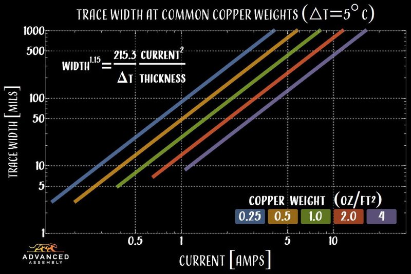
A 5°C delta T isn't a lot to play with at high operating temps.
As you can see, on 4 oz copper, you'd only want to run 10 Amps through a trace that's 500 mil wide. That's a lot of board area, and we're not every to 25 yet.
So one option is to put that current through multiple layers on your PCB.
Lets say you've got a 6 layer board.
A few different ways you could do it, but lets say you run power traces on layers 1, 3, 4, and 6 with ground returns for 2 and 6.
You'll have decent power integrity and the ground planes on 2 and 5 can help to dissipate the thermal energy.
Really though, at 75°C with a 5 °C delta T -- you need to do FEA or LEA.
Greg, I've scared them.
They've got quiet.
Come back Greg.
Let the light that you shine be seen!
 are there open source options for PCB analysis? not just for thermal analysis, but also for e.g. power system impedance?
![]() @Mark J Hughes - sounds good. Looking to distribute the power to multiple locations on the board and they will alternate which location is drawing the peak power over time. Will touch base when further down the design road.
@Mark J Hughes - sounds good. Looking to distribute the power to multiple locations on the board and they will alternate which location is drawing the peak power over time. Will touch base when further down the design road.
Never left sir!
@Christoph I'm sure there are, but I am not aware of any. I'll tell you who is though -- Dr. Eric Bogatin -- he's on a mission to find free tools for students.
@Christoph I've been trying to do some analysis like that with Elmer, which theoretically supports a bunch of relevant PCB physics, but isn't at all user friendly
@Jason Hey man -- we'd love to work with you.
![]() Just wondering if it would be possible to make a DIY process based on ultra-low-cost (2$ JLCPCB or so) standard PCBs like this:
Just wondering if it would be possible to make a DIY process based on ultra-low-cost (2$ JLCPCB or so) standard PCBs like this:
* Design board with no solder mask on actual (high-current) traces
* Add thin dummy traces (with solder mask) to connect all traces together
* Use electroplating to add extra copper to the traces, should only deposit copper on the traces (where there is no solder mask)
* Drill away dummy traces (might help to have a pre-drilled hole to center the drill bit, removing traces like that was pretty easy with the good old strip grid prototyping boards back in the days)
One potential problem I see with this is that the cheap PCBs will always come with some kind of plating (typically HASL), you can't opt out of this. Not sure if the electroplating process would work on top of the HASL (tin) finish.
@Christoph https://www.signalintegrityjournal.com/articles/2026-low-cost-and-free-tools-fit-for-an-engineers-personal-budget
@Jakob are you doing this for fun? Or trying to make something to market?
ooooh that looks like a good start. thank you
![]() Whoa, just had a crazy reflow idea that you "could" have the SMD component sit so high like a bridge that you could have other components underneath it. Very impractical but a fun show piece. That begs the question, what reflow considerations besides warp and proper pre-heating are needed for sitting so high off the substrate, if any?
Whoa, just had a crazy reflow idea that you "could" have the SMD component sit so high like a bridge that you could have other components underneath it. Very impractical but a fun show piece. That begs the question, what reflow considerations besides warp and proper pre-heating are needed for sitting so high off the substrate, if any?
@Jakob Simple answer is yes, but goes straight into the custom world. From a POC standpoint, it can be done.
![]() I'd do that for hobby projects only, for commercial projects it would probably be a lot more cost effective to just order a professional board.
I'd do that for hobby projects only, for commercial projects it would probably be a lot more cost effective to just order a professional board.
Yes, agree. But would be really cool to make!
@Jakob I'd still just buy it from someone. It's not worth the aggregation and setup costs.
*aggrevation.
![]() @Greg Ziraldo Would you expect any problems with electroplating copper on top of the HASL finish?
@Greg Ziraldo Would you expect any problems with electroplating copper on top of the HASL finish?
You mean like delamination?
Yes. You can expect that....if it even manages to stick in the first place.
![]() Yes. I know electroplating can be tricky depending on the combination of materials used.
Yes. I know electroplating can be tricky depending on the combination of materials used.
It's not just chemistry.
The crystal structure of the copper comes into play.
Getting copper to plate to other copper at a grain boundary is hard enough -- but with the HASL in the middle, I personally don't see it happening.
You would not be able to plate to HASL. There might be an electroless deposition, but not thru electroplating.
Maybe you can get some boards with OSP that you can clean before your experiment?
Alright -- what other heavy-copper questions do you have? It's not often that Greg Ziraldo is in your presence.
Three cheers for Greg Ziraldo.
Hip.hip.....
![]() I understand. Do you think an ENIG finish (with a few micrometers of gold on top) would work better if you want to electroplate copper on top of it? Still a lot cheaper than ordering a professional 4Oz/6Oz PCB.
I understand. Do you think an ENIG finish (with a few micrometers of gold on top) would work better if you want to electroplate copper on top of it? Still a lot cheaper than ordering a professional 4Oz/6Oz PCB.
@Jakob You need clean, unoxidized copper.
 I know it's not quite heavy copper, but I have a few questions on MCPCB tech
fair game?
Go for it.
I've seen two primary MCPCB tech available
First question is why do you want it?
copper - substrate - metal - substrate - copper
and copper - substrate - copper - substrate - metal
metal in middle vs. multilayer PCB laminated to metal
I'm always a fan of using balanced stackups -- otherwise differential coefficients of thermal expansion during reflow can cause warpage. Can't put flat parts on a curved surface.
One of the bugbears of my design existence has been a SSR for automotive use specced to handle 100-120A continuous
Now -- there are simulators that can allow you to balance that out. But most people don't have access to one.
100-120 continuous? Sheesh.
OTOH, with metal core, balanced implies "way more difficult via fabrication" no?
so far, the most successful PCB I've done with SMT parts had several pieces of .25" square copper placed on the board as busbar and soldered reflow style after an acid wash to improve sodlerability
You can certainly use a solid copper core or or "bottom layer" of the stack up. This would be for heat sink/thermal dissipation?
yeah, I used an osh part 2oz board with the extra busbar
What greg said -- just use copper pours on the opposite layer--doesn't have to be continuous.
Guess who makes OshPark's boards?
without the busbar, the 2oz board would get nuked in certain spots due to uneven current/thermal distribution
The designs that I have worked with have either defense/missile or down-hole drilling applications.
osh park? amitron in chicago
mostly
That's right. GREG-freaking-ZIRALDO!
Out of our Royal Circuits facility in Hollister, Ca.
the ones I got are 95% from Amitron in chicago
I order a lot of full panels from Osh and get drop ships from fab
All of a sudden it's an hour later! Greg, Mark, I assume you've got to get back to work? Those PCBs aren't going to quick-turn themselves, right?
Ah.
Well @Dave Blundell do me a favor and email me at mhughes@royalcircuits.com and we'll follow up one-on-one.
is there a compelling reason why PTH are never connected to MCPCB
 Thanks guys
thanks @Mark J Hughes will do
Discussions
Become a Hackaday.io Member
Create an account to leave a comment. Already have an account? Log In.