-
Transistor Mixer
11/22/2021 at 00:01 • 0 commentsThis article is about a simple transistor mixer circuit.
![]()
This device can be used for mixing audio samples that are used for make music, particularly techno. However, because the supply voltage is only 1.5 V it is very easy to saturate the output.
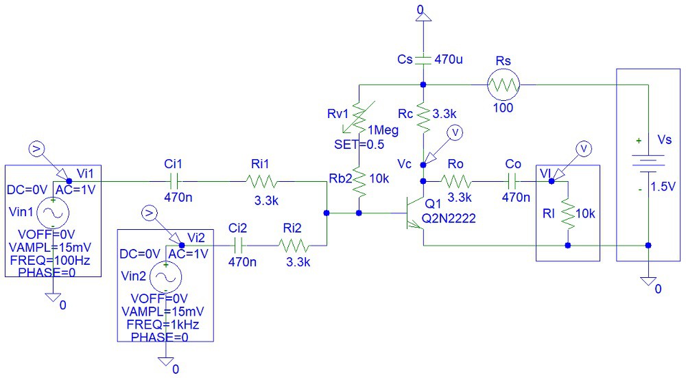
Step 1: Design the Circuit
The circuit was drawn via PSpice student simulation software version 9.1:
![]()
The input lower band pass frequency approximately equals to:
fil = 1 / (2*pi*Ri1*Ci1)
= 1 / (2*pi*3300 ohms*(470*10^-9 Farads))
= 102.614405604 Hz
The output lower band pass frequency approximately equals to (assuming the load is short circuit)
fol = 1 / (2*pi*(Rc+Ro)*Co)
= 1 / (2*pi*(3300 ohms+3300 ohms)*(470*10^-9 Farads))
= 1 / (2*pi*6600 ohms*(470*10^-9 Farads))
51.307202802 Hz
This frequency is a bit high. The lower band pass frequency supposed to be about 20 Hz. However, I was trying to avoid the use of electrolytic/bipolar capacitors.
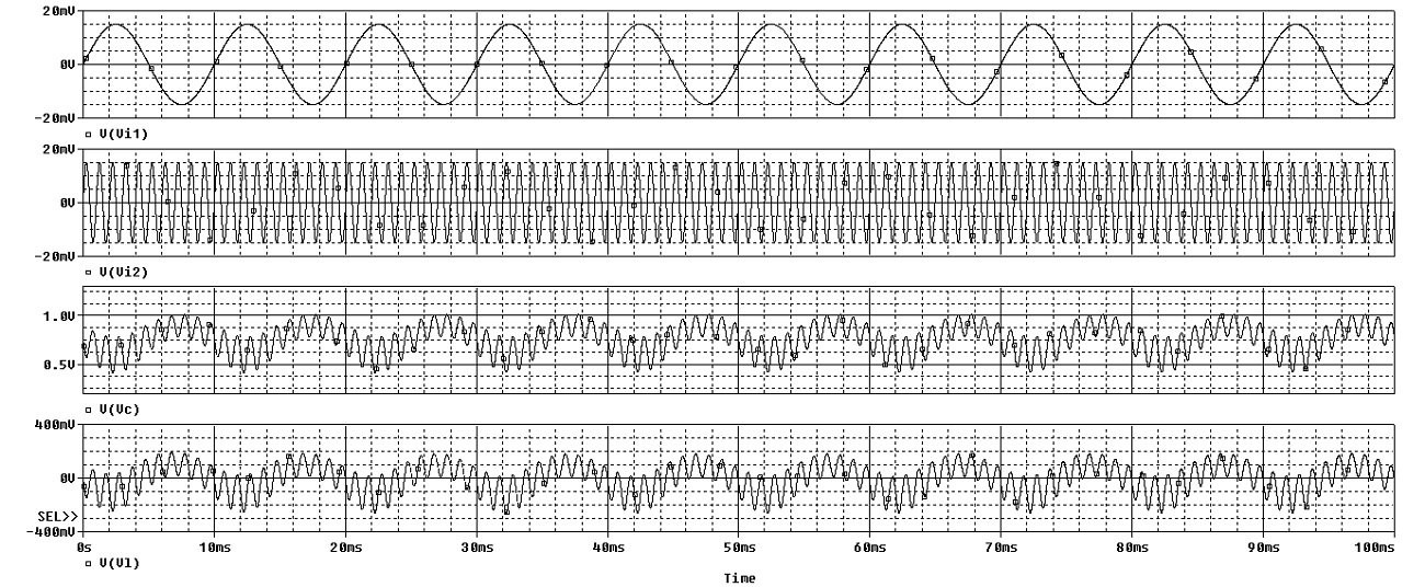
Step 2: Simulations
Simulations show that the transient response is amplified:
![]()
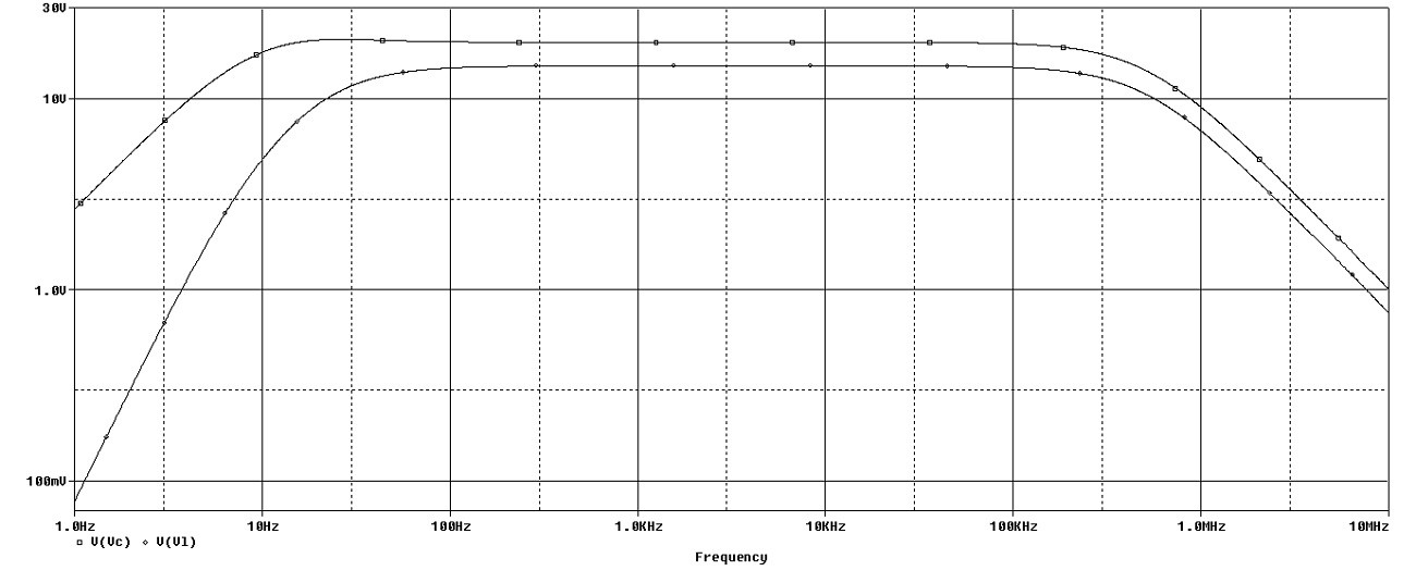
Frequency response:
![]()
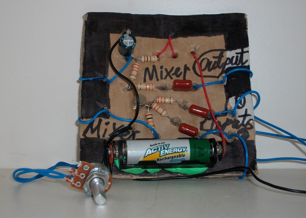
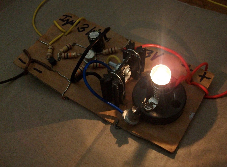
Step 3: Make the Circuit
I made the circuit on a piece of cardboard to avoid purchasing a matrix board:
![]()
Step 4: Testing
I used Instrustar USB Oscilloscope for testing.
In the plots below the green signal is the input and the red signal is the output.
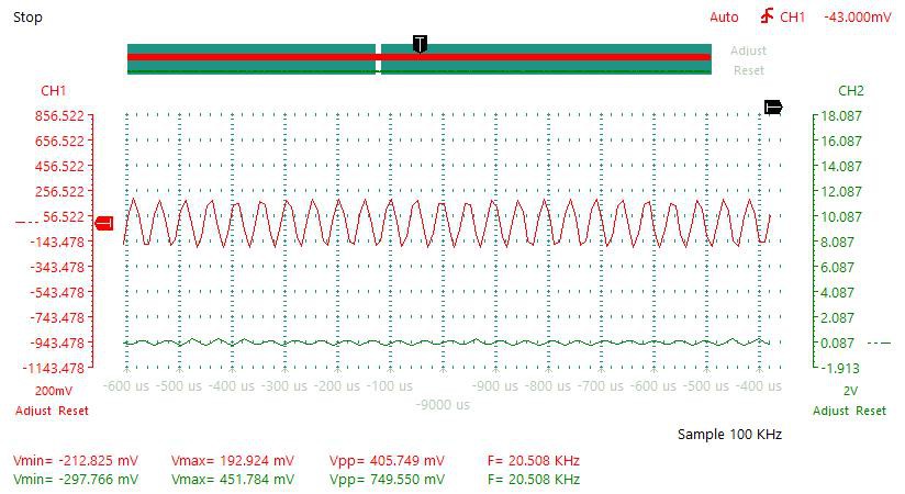
1 kHz Input Maximum Gain:
![]()
The gain is 810 mV / 187 mV = 4.33155080214
I placed additional resistors in series with Ri1 and Ri2 to prevent output signal saturation. Thus the actual gain is a lot higher than the calculated value of 3.44155.
Gain can be increased by reducing Ri1 and Ri2 resistors values and at the same time increasing the Ci1 and Ci2 capacitors (to prevent the rise in lower band pass frequency).
20 Hz Input:
![]()
20 kHz Input:
![]()
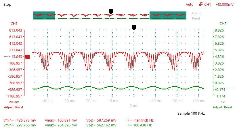
Distortion 1:
I varied the variable resistor to create distortion effect:
![]()
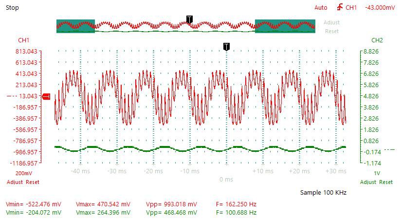
Distortion 2:
![]()
Summation:
![]()
Conclusion
This simple transistor mixer only need one 1.5 V AA or one 1.5 V AAA battery to work.
-
Touch Light Bulb
06/23/2020 at 09:39 • 0 commentsThis article is based on the following designs that gave me an idea:
https://www.instructables.com/id/MOSFET-Touch-Lamp/
https://www.instructables.com/id/Touch-Lamp-1/
https://www.instructables.com/id/Recycled-Components-Touch-Lamp/
The designs above show a low current LED driver. A typical LED needs only 10 mA. However, a typical 1.5 V light bulb needs 300 mA. I modified the circuit to drive higher current loads by adding an extra transistor.
![]()
You can see my circuit working in this video:
Step 1: Design the Circuit
I modified the design in the links above by adding an extra transistor in the cascaded transistor amplification system. My design is a bit similar to:
https://www.instructables.com/id/Touch-Lamp-1/
![]()
You do not need 3 V power supply and you do not have to use Darlington pair transistors.
You design for 1.5 V power supply with two NPN and two PNP transistors (similar to: https://www.instructables.com/id/Touch-Lamp-1/) or 3 V power supply and use four NPN or four PNP transistors (similar to: https://www.instructables.com/id/Recycled-Components-Touch-Lamp/).
However, you must use a heat sink for the transistor that will drive the light bulb.
Determine Darlington pair transistor saturation voltage:
Vce3saturation = Vce3a + Vbe3b
= 0.2 V + 0.7 V = 0.9 V
Use of Darlington pair reduces the amount of components in the circuit but high saturation voltage (eg. 0.9 V instead of 0.2 V) increases the transistor power dissipation:
Pt = Vce * Ic
Calculate the minimum Q3 transistor current gain to ensure saturation:
Beta3Min = Ic3 / Ib3 = 0.3 A / ((Vs - Vce2 - Vbe3) / Rb3)
= 0.3 A / ((3 V - 0.2 V - 2 * 0.7 V) / 1000 ohms)
= 0.3 A / (1.4 V / 1000 ohms)
= 214.285714286
(this is a very low minimum gain for a Darlington pair transistor)
Calculate the minimum Q2 transistor current gain to ensure saturation:
Beta2Min = Ic2 / Ib2 = (((Vs - Vce2 - Vb3) / Rb3) + ((Vs - Vce2) / Rc2)) / ((Vs - Vce1 - Vbe2) / Rb2)
= (((3 V - 0.2 V - 2 * 0.7 V) / 1000 ohms) + ((3 V - 0.2 V) / 10,000 ohms)) / ((3 V - 0.2 V - 0.7 V) / 10,000)
= ((1.4 V / 1000 ohms) + (2.8 V / 10,000 ohms)) / (2.1 V / 10,000)
= 8
(a typical minimum gain for a general purpose transistor is 20)
Calculate the minimum Q1 transistor current gain to ensure saturation:
Beta1Min = Ic1 / Ib1 = (((Vs - Vce1 - Vbe2) / Rb2 + ((Vs - Vce1) / Rc1)) / ((Vs - Vbe1) / (Rb1 + Rhuman))
= (((3 V - 0.2 V - 0.7 V) / 10,000 ohms + ((3 V - 0.2 V) / 100,000 ohms)) / ((3 V - 0.7 V) / (100,000 ohms + 1,000,000 ohms))
= ((2.1 V / 10,000 ohms) + (2.8 V / 100,000 ohms)) / (2.3 V / 1,100,000 ohms)
= 113.826086957
If the resistance of a human is only 100 kohms then:
Beta1Min = ((2.1 V / 10,000 ohms) + (2.8 V / 100,000 ohms)) / (2.3 V / 200,000 ohms)
= 20.6956521739
Neither Q1 or Q2 transistors need to saturate for the circuit to work. They can just amplify the current. Transistor saturation does reduce the power dissipation. However, the first two transistors are not dissipating high currents and thus not high powers.
The Rs1/Cs1 and Rs2/Cs2 power supply low pass RC filters are used to filter power supply oscillations. Those oscillations could be due to 50 Hz/60 Hz main frequency noise or possible power supply oscillations that can occur even if you are powering the circuit with a 3 V battery source (two AA/AAA/C/D batteries in connected series). Those oscillations are caused by power source internal resistances.
Calculate the frequency of the low pass power supply filter:
fl1 = 1 / (2*pi*Rs1*Cs1) = 1 / (2*pi*100 ohms*(470*10^-6 F))
3.38627538493 Hz
You can try using Rs2 of 1 kohms and Cs2 of just 47 uF. The low pass frequency will be the same:
fl2 = 1 / (2*pi*Rs2*Cs2) = 1 / (2*pi*1,000 ohms*(47*10^-6 F))
3.38627538493 Hz
However, this will reduce the loading affect on the first power supply filter made from Rs1 and Cs1 resistors.
Step 2: Make the Circuit
I only used a soldering iron for the power Darlington pair transistor. I used TIP122 transistor....
Read more » -
Transistor Modulator
03/30/2020 at 04:40 • 0 commentsThis paper describes a modulator made from four transistors.
This circuit is basically a voltage controlled amplifier (VCA) connected to sine wave generator that modulates the input frequency. Nowadays there are voltage controlled amplifier ICs (integrated circuits) and complete circuits sold online.
However, this circuit works at voltages as low as 1.5 V.
There is another cheaper and simpler circuit on this website. However, that circuit that only allows basic nonlinear modulation:
https://hackaday.io/page/7004-simple-transistor-modulator
Step 1: Design the Circuit
I have drawn the circuit in the old PSpice software:
![]()
The 50 Hz modulator frequency is 20 times smaller than the 1 kHz circuit input frequency. Thus the signals would not overlap in the frequency domain.
I used a current mirror source to ensure a constant and temperature independent current supply to Q1a and Q1b transistors because it is the current that controls the differential amplifier AC voltage gain.
The differential voltage gain is equal to:
Gain = Vc / Vi = Beta*Rc2 / (2 * Beta * re + Ri1 + Ri2) = Rc2 / (2 * Vbe / Ie + (Ri1 + Ri2)/Beta)
(We ignore the biasing resistors Rb1 and Rb2 because they take very little current from input)
= Rc2 / (2 * Vbe / ((Vs - Vbe2) / Rm / 2) + (Ri1 + Ri2) / Beta)
= Rc2 / (4 * Vbe / ((Vs - Vbe2) / Rm) + (Ri1 + Ri2) / Beta)
= 1000 ohms / (4 * 26 mV / ((1.5 V - 0.7 V)/1000 ohms) + 1000 ohms / 100 + 1000 ohms / 100)
= 1000 ohms / 150
= 6.66666666667
For 30 mV input the output should be
Vc = Vin * Gain = 30 mV * 6.66666666667 = 200 mV or 0.2 V
Step 2: Simulations
The graph below is showing that the modulator is working.
![]()
The graph above shows the voltage controller amplifier gain output is swinging from 250 mV to 100 mV amplitude. Thus the average output amplitude is 175 mV that almost similar to the 200 mV that was predicted in the calculations. Discrepancy was caused by differences in transistor models parameter values used in the PSpice software and the model parameters values that I used in the calculations. Those parameters include the Beta value and the 26 mV input AC Vbe (AC base emitter) voltage.


 Fabricate.IO
 Jon Klein
 Tony
Tony krtkl
krtkl Tim Wilkinson
 Dmitry
 Laetitia BEL
 Neo
Neo opit
opit Foaly
Foaly Voja Antonic
 Joseph Prosnitz
 Roman Weitendorf
 Daniel Knezevic
 ActualDragon
Hi,
It was a great method of calculation, I liked the method of fine detailing and it is a professional method that avoids you from making math mistakes.
Good luck and Keep going!
Abdul