 Christoph
 Antti Lukats
 Aleksandar Bradic
 Bud Bennett
 Sophi Kravitz
-
Text-in-pad from gerbers
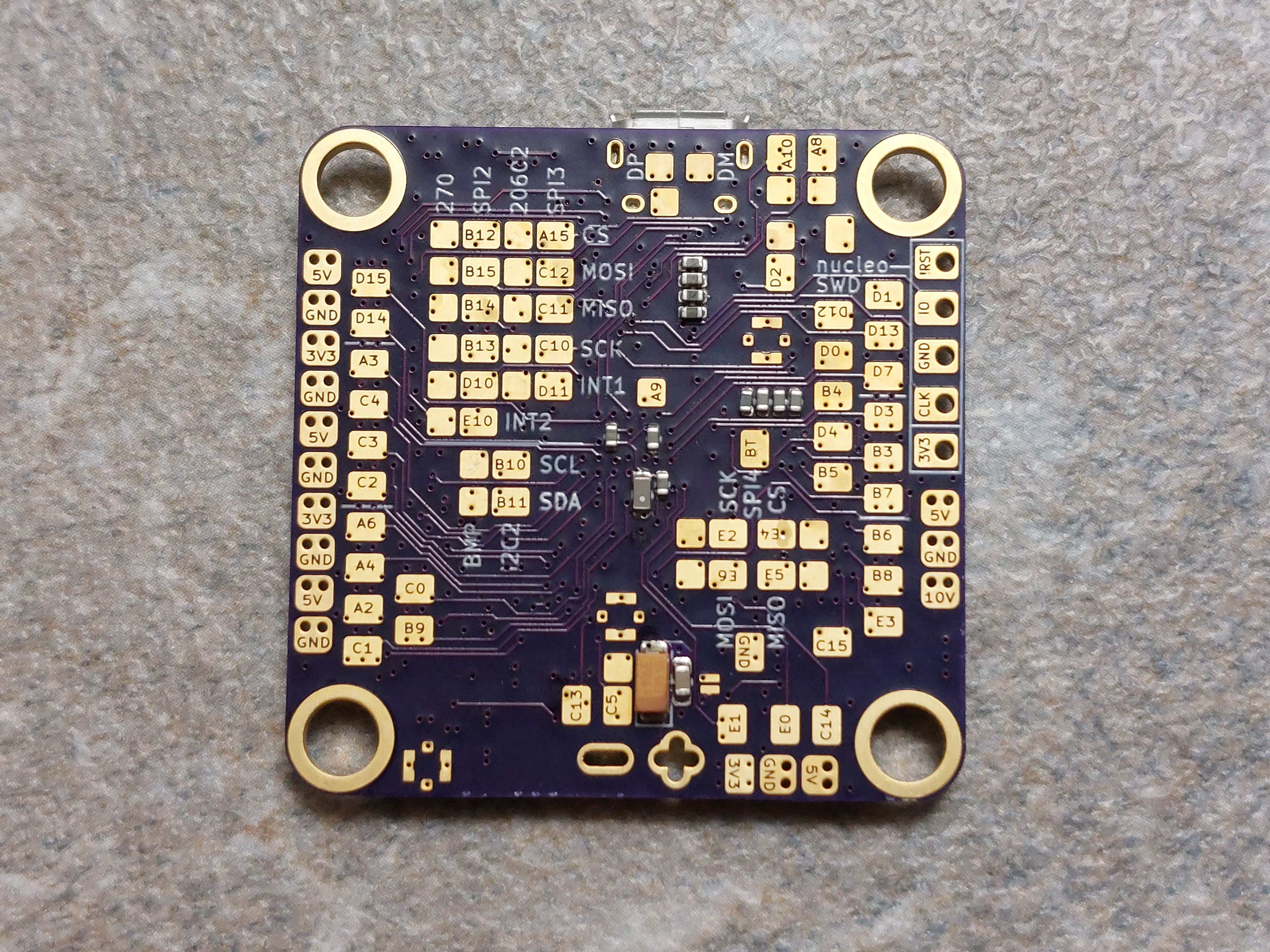
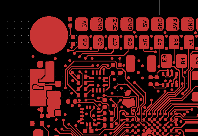
03/23/2023 at 22:55 • 4 commentsI recently posted some pictures of a PCB with text in pads describing their purpose (for example "5V", "GND" or "A9"):
![]()
And I received lots of questions about the process, so here's a little tutorial.
A quick overview:
- Some preliminary remarks
- Prepare the layout
- Produce raw gerber files
- Subtract text from copper using gerber_combine
- Check
- Enjoy
Preliminary Remarks
Of course there were some comments on this technique after I published this page. Here are the most important concerns:
- While a label-in-pad is useful for finding a pad before you solder to it, the information is invisible afterwards.
- Difficult to probe. You can touch a dead spot in a character's center and get no electrical connection
- Solder residue gets trapped between pad voids and joint
Silk screen is still the better way to label things. I'm not recommending this technique over silk screen. For eye candy in hobby projects it's probably fine.
Layout preparation
- Make sure that your pads actually allow for embedded text! That means that the pads must be large enough and that they don't have vias where the text would be. That sounds simple, but can sometimes be difficult to achieve. Don't sacrifice electrical functionality for eye candy.
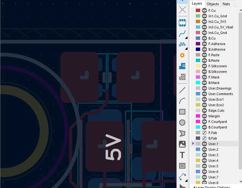
- Place the labels you want in your pads on an extra layer. KiCad has user layers for this.
Example (text height: 0.5 mm; text width: 0.6 mm; line width: 0.1 mm):
This text (or any other features you draw on that layer) will later be subtracted from the copper layer, so the end result will have better resolution than silkscreen. The silkscreen design rules don't apply here.
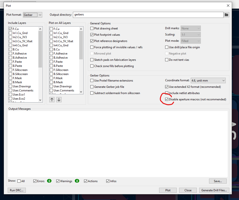
Producing the raw gerber files
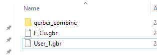
Nothing too special, but gerber_combine requires aperture macros to be disabled. So produce your gerber files without aperture macros. KiCad plot example:
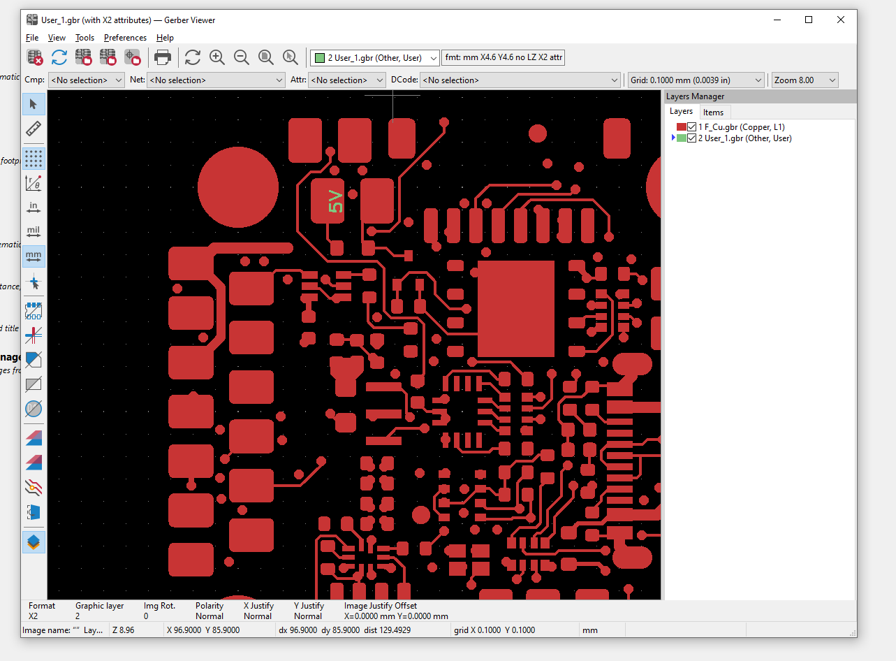
Plot copper layers and the text layers you want to subtract from those copper layers (here: F.Cu and User.1; the latter is not visible in the screenshot above). Check the raw output with a gerber viewer:
Subtract text from copper using gerber_combine
Get the gerber_combine python script from here: https://github.com/bobc/kicad-utils/tree/v5/scripts/gerber_combine and put it into the folder where your gerber files reside. Could look like this;
Open a terminal and enter the gerber_combine folder. Then use gerber_combine to subtract the layers from each other:
python .\gerber_combine.py -a ..\F_Cu.gbr -s ..\User_1.gbr -o ..\result.gbrLet's have a look at the result:
Enjoy
The pads still survive desoldering, just like pads that don't have text in them. Nothing has changed fundamentally:
![]()
-
Diving into SCPI
09/10/2022 at 19:41 • 0 comments![]()
Setting up instruments (like an oscilloscope or a signal generator) can be quite tedious. For me, that is when
- I have to set up two devices or more
- it has to be done repeatedly
The second point has (at least) two flavors:
- either because I need to measure, tweak the device under test, and get back to it later
- or because I have to test a device in different fixtures with different setups, going back and forth
Until now I thought that controlling them via USB or LAN would be quite a steep learning curve, but one day I was just so fed up with all that button pushing (especially when the rotary knobs jump over to the next value when you push...) that I gave it a try. And it was easier than I thought!
Simple test
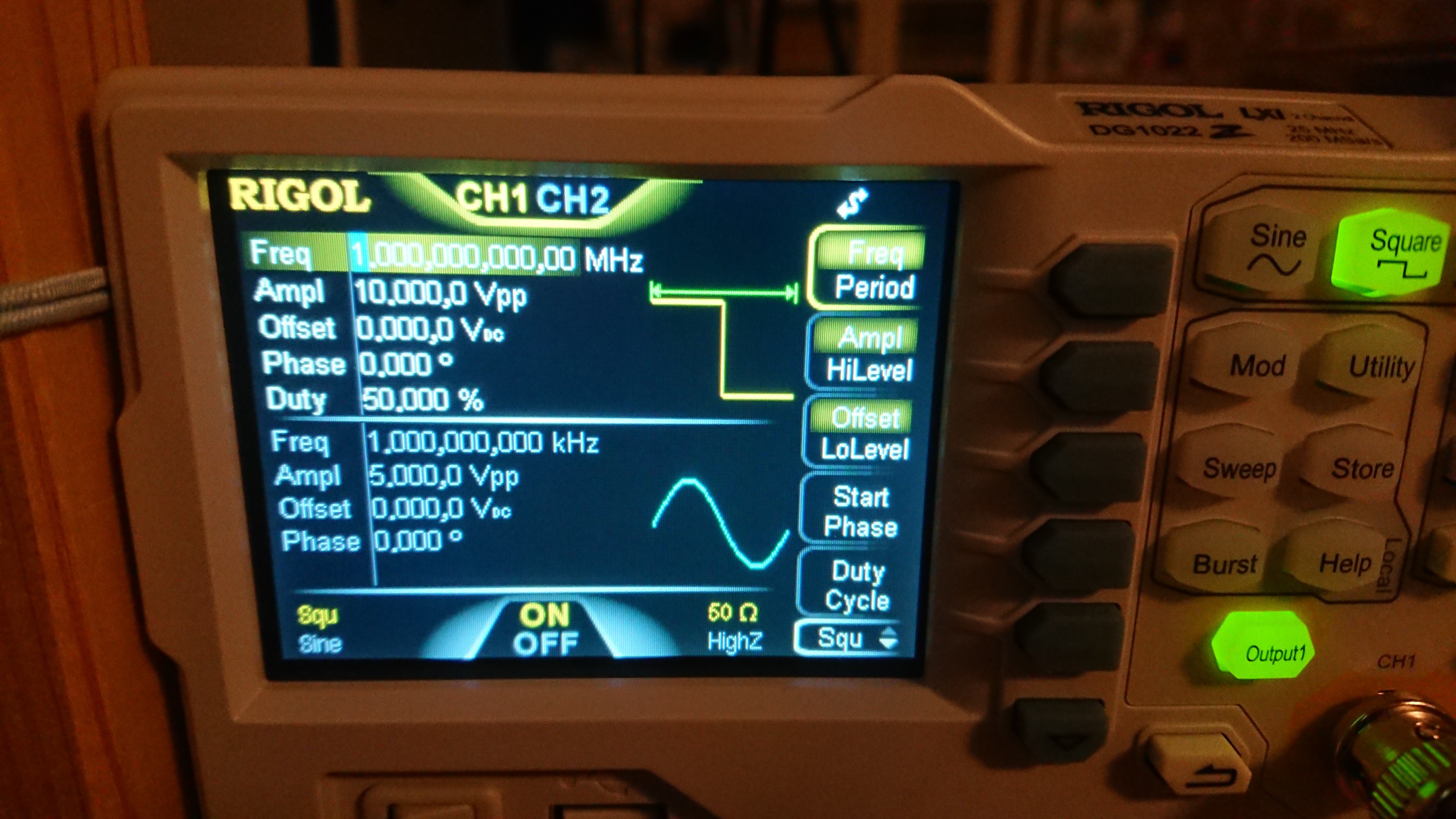
As a simple test, I configured a signal generator (Rigol DG1022Z) to output a 1 MHz, 10 Vpp square wave into a 50 Ohm load, and the scope accordingly. Both instruments are connected to my computer via USB, and I'm using pyvisa to control them with a python script.
The signal generator feeds its output into a coax cable which is terminated with 50 Ohm on the scope side.
pyvisa offers a resource manager that can discover instruments:
import pyvisa as visa
rm = visa.ResourceManager()
# let's see what we have connected:
rm.list_resources()
The output of list_resources containts a string for each instrument that was found, and this string includes an instrument's serial number, like so:
'USB0::6833::1602::DG1ZA23530xxxx::0::INSTR'
So we can go through that list and look for a specific instrument:
resources = rm.list_resources()
for i in range(len(resources)):
    r_name = resources[i]
    if (r_name.split("::")[3] == DS1054_Serial):
        # now do something with the instrument
To do something with the instrument, it must be opened before we can send commands or query values.
Example: reset the instrument
instr.write("*RST")Starting with a freshly reset instrument, it's just a matter of looking up the correct commands in the instrument's programming manual and writing them all down:
import pyvisa as visa
import sys
rm = visa.ResourceManager()

DG1022_Serial = "DG1ZA23530xxxx"
DS1054_Serial = "DS1ZA20180xxxx"

rm.list_resources()

resources = rm.list_resources()

scope_done = False
siggen_done = False

# find scope, reset to defaults and apply only those changes that deviate from those defaults
for i in range(len(resources)):
    r_name = resources[i]
    if (r_name.split("::")[3] == DS1054_Serial):
        instr = rm.open_resource(r_name)
        # resourceReply = instr.query('*IDN?').upper()
        # timebase
        # Ch1 coupling AC/DC
        # Ch1 attenuation
        # Ch1 V/Div
        # trigger
        # run
        instr.write("*RST")
        instr.write("TIM:MAIN:SCAL 50e-9")
        instr.write("CHAN1:COUP DC")
        instr.write("CHAN1:PROB 1")
        instr.write("CHAN1:SCAL 2")
        instr.write("CHAN1:DISP ON")
        scope_done = True

if not scope_done:
  print("Could not find scope. Check connection and retry.")
#  exit()

# find signal generator, reset to defaults and apply only those changes that deviate from those defaults
for i in range(len(resources)):
    r_name = resources[i]
    if (r_name.split("::")[3] == DG1022_Serial):
        instr = rm.open_resource(r_name)
        # resourceReply = instr.query('*IDN?').upper()
        instr.write("*RST")
        instr.write(":OUTP1:LOAD 50")
        instr.write(":OUTP1:IMPEDANCE 50")
        instr.write(":SOURCE1:APPL:SQU 1e6,10")
        instr.write(":OUTP1 ON")
        # instr.control_ren(visa.constants.RENLineOperation.address_gtl)
        siggen_done = True

if not siggen_done:
  print("Could not find signal generator. Check connection and retry.")
#  sys.exit()

print("All done.")
The signal generator has a little caveat. Once the setup via USB is done, it remains in "remote mode", and the buttons can't be used. We can see that it's in remote mode when there is a little arrow symbol in the top right corner:
![]()
That's inconvenient if further tweaks are to be done with the buttons. Instead, it shows a message
Instrument is locked for VISA,
Press the "Local" to unlock.
However, there...
Read more » -
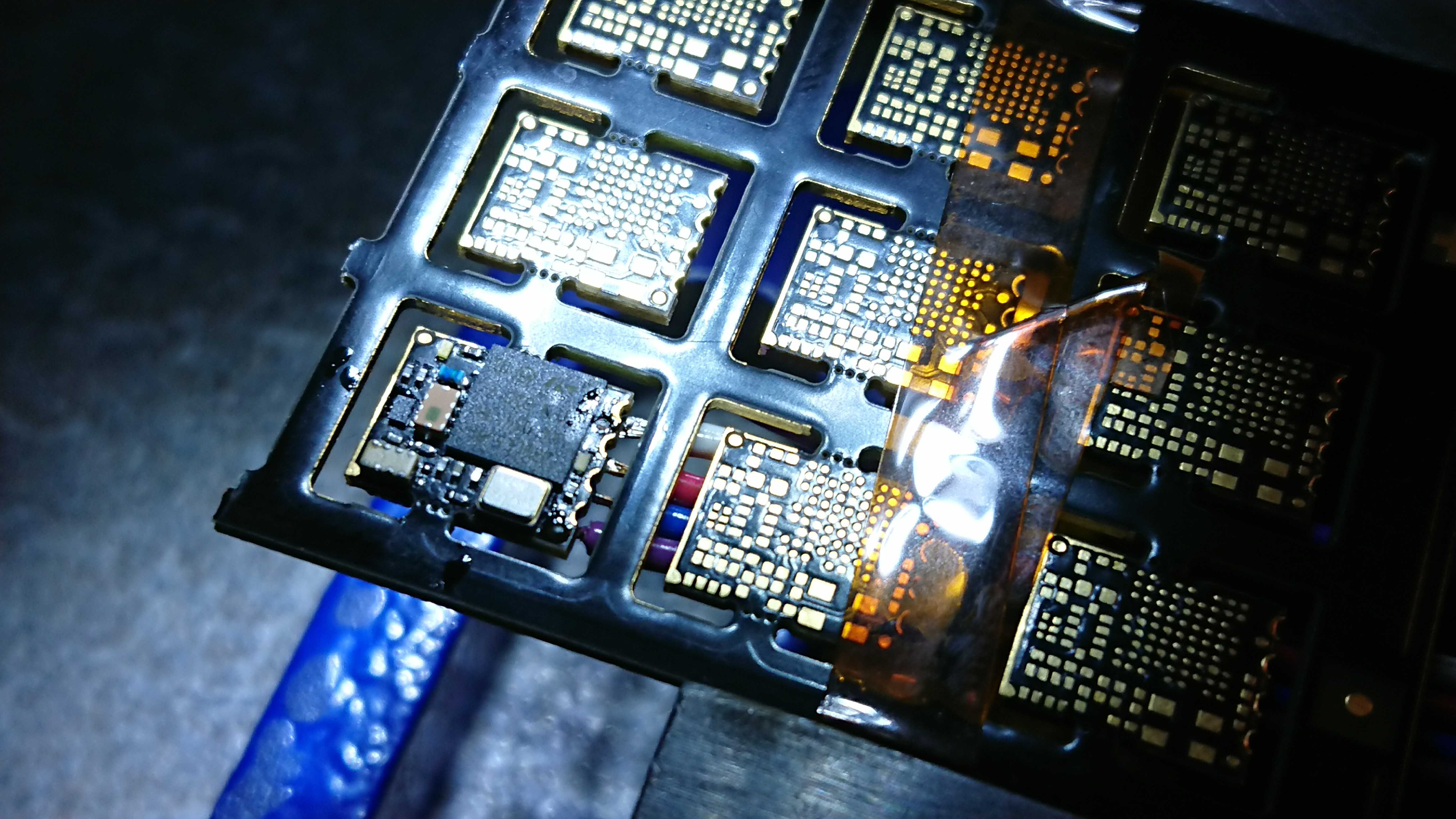
Assembling densely populated PCBs with 0201 components
05/30/2021 at 22:07 • 0 commentsI recently assembled a tiny 7.5 x 9.5 mm PCB (actually two) with 0201 passives, LEDs, a BGA and a nasty LGA. Components on both sides. It was difficult, and I was not sure if could do it, but it went well with the right tricks and some experimentation.
TL;DR: the result:
![]()
So how did I get there?
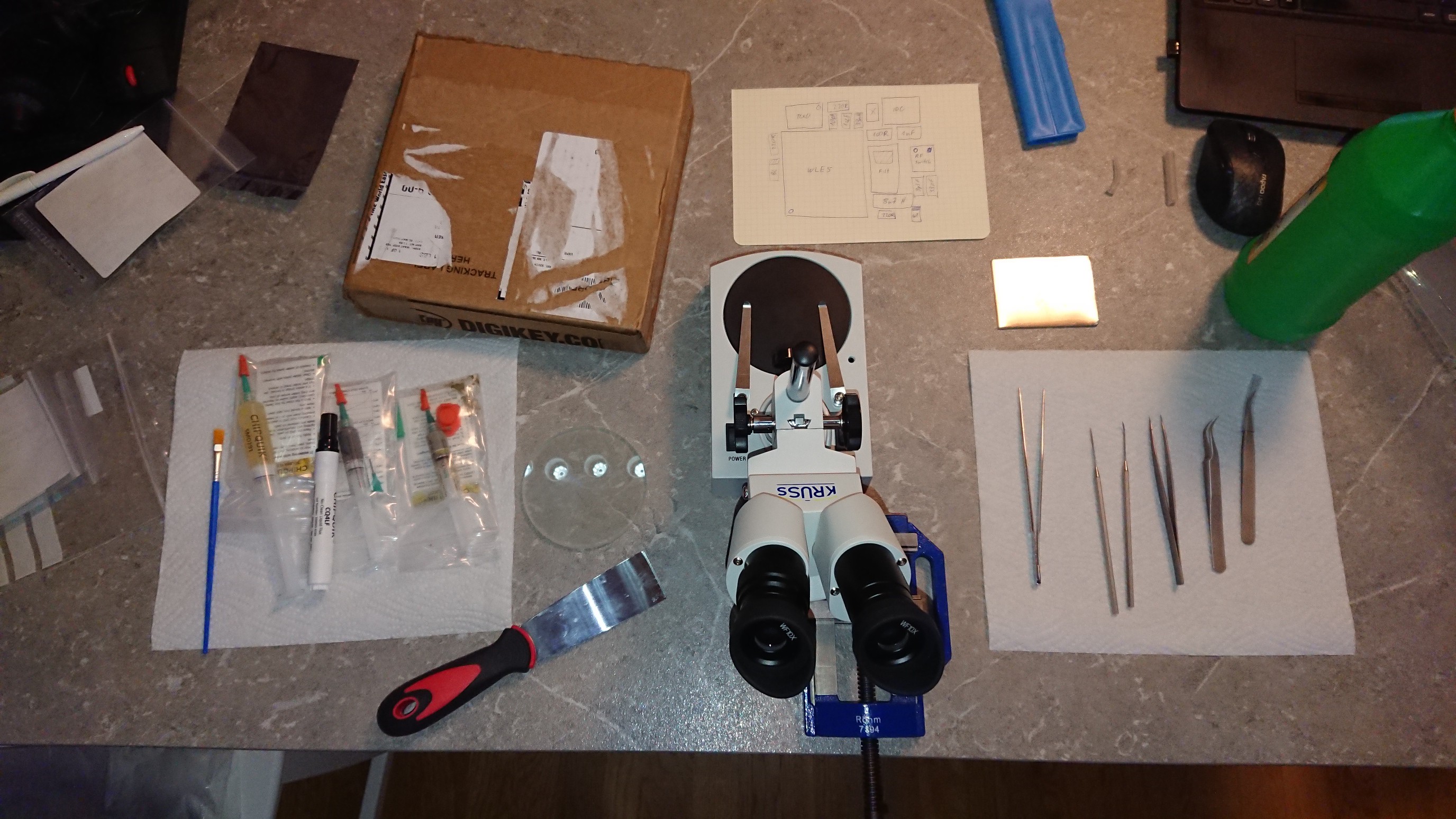
Tools and helpers
A lot of little tools and helpers are needed, and I'll try to include everything here. First of all - for lack of a dedicated bench - I assemble my boards in the kitchen. That means that I have to keep my kitchen tidy to cut down the time it takes to convert between food and PCB output. Same for my assembly equipment:
![]()
- stereo microscope. I use 10x magnification and that's enough for 0201
- a heavy vise
- those pointy dentist things (I use them to apply paste, flux gel, and poke parts)
- tweezers
- a squeegee to spread paste/flux gel
- a small glass plate for a blob of solder paste and flux gel
- a small aluminium plate
- soldering iron
- hot air station
- a soft brush to apply flux gel and to clean the PCB
- solder paste, low temp SnBi and high temp SnAg
- tacky flux gel and a flux pen
- alcohol (isopropyl is recommended but I use ethanol) for cleaning the PCB and a flat container that you can rinse the PCB in
- some paper towels to clean tools and the PCB
PCB Preparation
Not that complex. I clean the PCB with ethanol and prepare a cheat sheet with part location, value and orientation for both sides.
Bench Preparation
As in the picture above, I put all my tools in approximately the place where I need them. I put a blob of solder paste (each type) and some tacky flux gel on the glass plate. The flux gel is spread with a squeegee to give me a thin, even layer of flux. The idea is that I can pick a part with tweezers, place it on the tacky flux layer, and as a result have a part with flux on the bottom, but not everywhere else.
Adhesion is always higher between tweezers and part than it is between part and PCB. That's a law.
BGAs and other high temp stuff first
I solder high temperature components first. Since BGAs already come with the right amount of solder in the right place (good!), we can't pick the type of solder in this case. It's most probably high temp SnAg solder, and if it's something different, you'd probably know that.
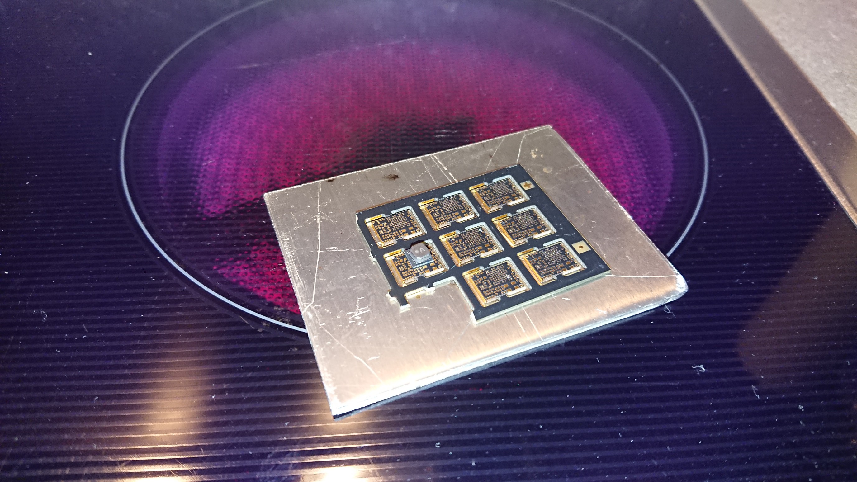
The BGA is dipped in the tacky flux layer and placed on the PCB. The solder mask helps figuring out if it's placed correctly: I place a heavy part on top to get some pressure between the solder balls and the PCB. Then I can feel it "snap" into place in the solder mask openings. the extra weight stays on during soldering. The solder's surface tension is pretty high, so the extra weight won't squash the joints.
I solder BGAs on a hot plate, which is conveniently included in pretty much every kitchen worth its name:
![]()
That's an STM32WLE5, with a 4x4 mm inductor on top. Here you can also see what the aluminium plate is used for. It spreads the heat and doesn't allow radiated heat from the heater reach the PCB. That's a thing because these glass ceramic plates transmit infrared radiation, and the aluminium plate will block that. Turn it to max and wait until the solder reflows. And extra blob of high temp paste somewhere on the PCB helps to see when reflow temperature is reached Then switch the plate off, wait 10 to 20 seconds and slide the whole thing (alu + PCB) off the hot plate.
Other typical high-temp parts are connectors. I do these with SnAg for its higher mechanical strength. This PCB has a u.Fl connector on the bottom that I solder with an iron and normal SnAg wire in the vise. One pad first, align the part, then solder the rest.
Parts with small pads will require something other than wire. In that case, I pre-tin the pads with paste and an iron, apply some flux again, and then reflow the pre-tinned pads with hot air to level them. Touch up until all pads for a given part have solder pillows of roughly the same height. That's right, no stencil!
Clean the PCB with alcohol to get rid of excess paste...
Read more »
This user joined on 05/04/2014.


My Projects
Projects I Contribute To
My Pages

Projects I Like & Follow
 Reinier van der Lee
 Alex Klimaj
 timonsku
 alpha_ninja
 Jenny List
Acquire EEG, ECG, EMG (medical instrument) signals while rejecting AC coupled noise
 Paul Stoffregen
 Kumar, Abhishek
 jaromir.sukuba
 David
David PointyOintment
 Philipp Klaus
 deʃhipu
 SUF
SUFShare this profile
ShareBits


Christoph
wrote 02/26/2019 at 08:09
•
point
Not any more. Lost some hair since that picture was taken

Daren Schwenke
wrote 02/26/2019 at 17:14
•
point
Not ideal, but you still have the rest of the required., and you are a hacker.. You come from the land of the ice and snow, from the midnight sun, where the hot springs flow... the hammer of the gods. You'll drive your ships to new lands, to fight the horde, and sing and cry. Valhalla, I am coming!
Dude... you need to do a Thor armor project. You would be perfect. :)