-
Network Analyzer - Repair
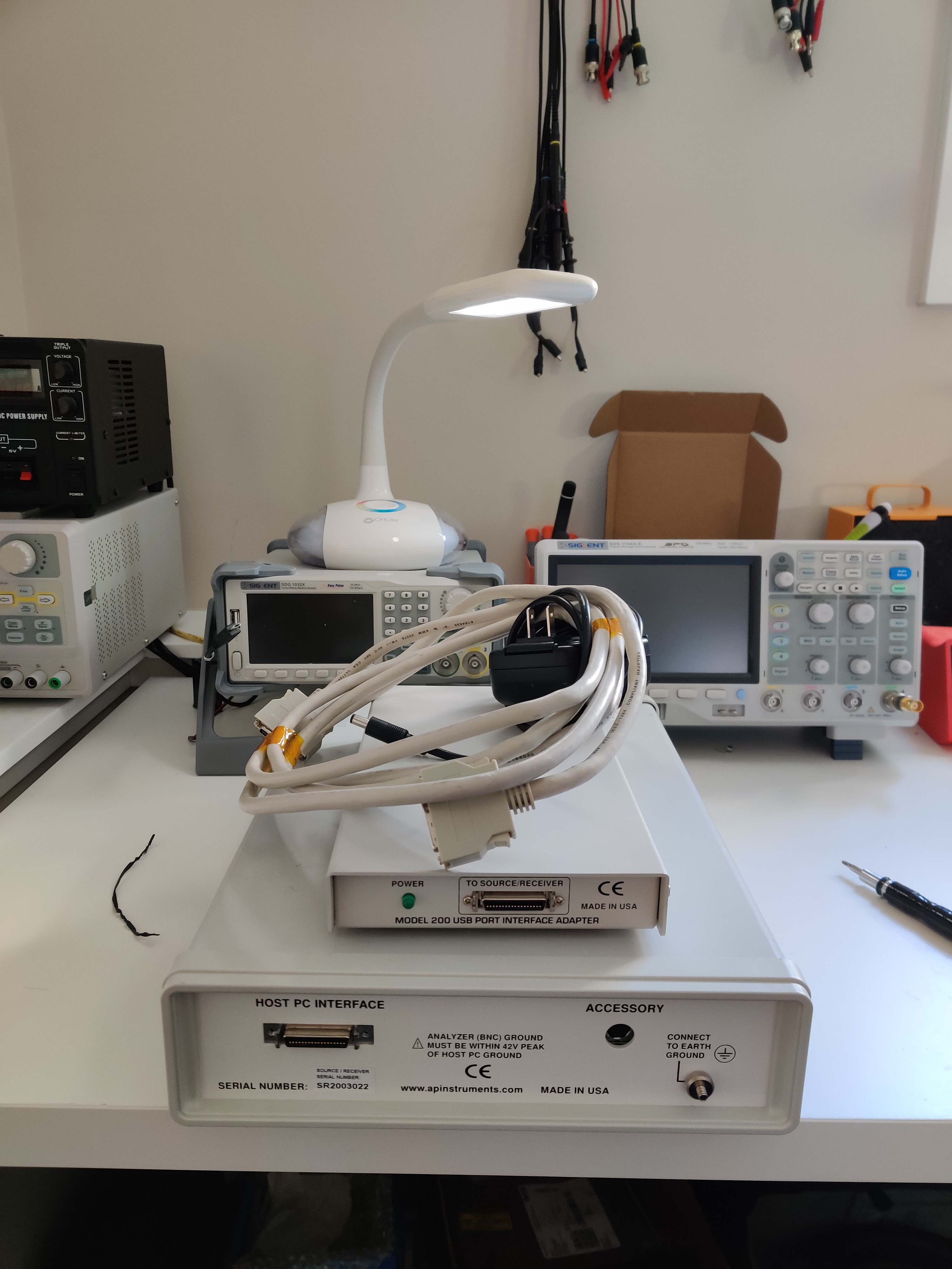
06/15/2023 at 22:34 • 0 commentsI’ve got an AP instruments network analyzer that stopped analyzing. The system is comprised of a USB interface adapter and a main unit. The only symptom is the absence of a power LED on the main unit.
![]()
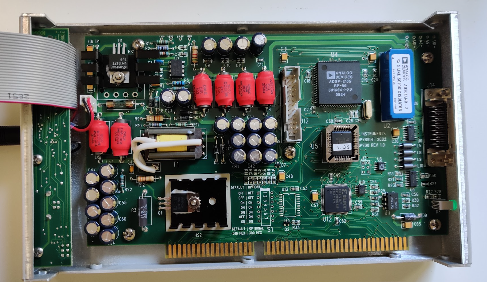
Instead of checking continuity of the cable, (because who am I kidding that’s no fun) I decided to open up the interface adapter.
![]()
Luckily, they gave us nice test points we can check right off the bat. All the low voltage rails (12V, 5V, 3V3) look good… but the one’s near the main connector are all zero volts. Maybe it waits for a PG signal before enabling 18V, +7V, -8V.
![]()
![]()
Next, I did some poking around the board. Seems like one of the main switchers is a UC3845N. VREF and VCC look good, but the switching node "OUTPUT" is held at GND. I’ll dig a bit deeper to see what the other pins are at.
![]()
After poking the other pins, it looks like COMP is being used to disable the device. Its being held low (ish) which is stopping the device from starting. Here’s a blurb from the datasheet. This COMP pin is being held low by a XILINX chip…. ☹. That complicates things.
![]()
I’m not sure what this chip needs before it will enable the main switcher. Checking the cable, I confirmed that the 12V, 5V, 3V3 rails are NOT sent to the main unit. This means the XILINX chip isn’t waiting for a handshake from anything on that unit (since it won’t be powered).
The suspect chip is a CPLD (XILINX XC9572XL). This isn’t something I can debug.... er atleast not easily.
THE FIX???
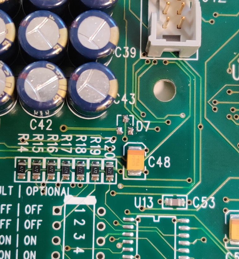
My plan is to remove the XILINX's ability to disable the switcher. Luckily there's a diode leading to COMP, so I can simply remove it (D7) and the switcher should work... what's causing the XILINX chip to assert this disable pin though?
![]()
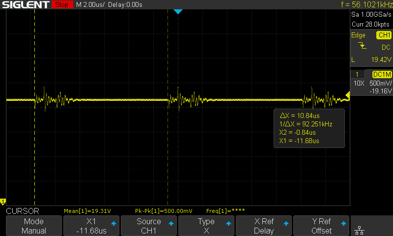
And voila, we have voltages. Nothings too accurate, but I was suspicious it wouldn’t be. Shown below is the +18V rail.
![]()
Now I’ll try plugging it in, but first I need the software to try and talk to it.
All seems happy. I can’t test the full feature set (I need more BNC cables), but I can at least see that the system is talking ect. I’ll do a final test tomorrow in the lab. (Tested and looks good).
![]()
-
Unpowered Digital Isolator Behaviour - ADUM348x
12/10/2022 at 22:45 • 0 commentsOverview:
I was recently working on a schematic that includes some digital isolators (ADUM3480). For power sequencing reasons, I need to operate the chip with the input side powered while the output is unpowered. My concern is… will the signals couple through from the input (powered side) to the output (unpowered) side?
The datasheet (here) doesn’t clearly define this quasi-unpowered behaviour, so I thought it best to do some testing. And, while I’m at it, I may as well document my findings.
![]()
TLDR:
If the output is unpowered, then no notable activity will be observed at the output, regardless of what signals are being sent at the input side.
The general test setup / procedure is as follows:
- Configure device on breadboard… 100nF decoupling for all PWR pins. V_{DDL1}, V_{DDL2}, V_{DD1}, V_{DD2}, V_{DDC1}, and V_{DDC2}.
- Tie all unused inputs to GND_{1} via a 10kohm resistor
- Power input V_{DDL1} and V_{DD1} at 3.3V to 5V, and power output V_{DDL1} and V_{DD1} at 3.3V to 5V
- Apply square wave to one input channel V_{Ix}
- Observe all pins on output (isolated side)
- Disconnect the output power from V_{DDL2} and V_{DD2} and repeat step 4/5
Test gear used:
- Isolated PSU – BK Precision Model 1670 DC Power Supply (3 isolated channels)
- Function Gen – SDG 1032X
- Oscilloscope – SDS 1104X
Results:
The initial sanity check confirmed the chip was functioning normally (step 3 to 5). The 3V3 input signal, and 5V output are shown below. Note these two signals couldn’t be captured in the same image since I don’t have isolating probes… and I didn’t want to short the two isolated GND’s.
Figure 1 - Input signal
![]()
Figure 2 - Output Signal
![]()
Next, I disconnected the 5V supply at the output, while leaving the input 10kHz square wave on V_{IB}. The output channel V_{OB} is shown below. We can see minor activity at the output (periodic spikes), likely caused by capacitive coupling.. since these spikes correspond to the edges of the input signal.
Figure 3 - Input Powered, Output Unpowered, Output signal
![]()
Next, I repeated the test with an input voltage of 5V, hoping to provide a worst case for capacitive coupling. There was a negligible change from the 3V3 test.
Caveats of these results:
Reminder that this test was conducted without any forced potential difference across the isolation barrier. I'm not sure how a 1kV difference between GND_1 and GND_2 might affect these results. I would think the results would be much the same, but I'm not very well versed in high voltage design.
This user joined on 01/06/2022.


 Bud Bennett
 spencerkrit78
 Reimu NotMoe
 benw
benw Shranav Palakurthi
 Ian Dunn
 Tim
Tim Adrian Studer
 Bluebird Labs Doug Peters
 Mangus Tiranus
 ElectronicABC
 LorneChrones (Nick)
 Keenan Rebera
 aiscope
 TheMixedSignal
 Stefan Wagner