 Elena Smith
Initially, electronic components were available in DIP packages only and PCB boards were used to be large-sized, thus having more space for the PCB wirings/connections. But with the research in nanotechnology, electronics get introduced with SMD(Service Mount Device) components. SMD components are very small-sized components and their sole purpose is to reduce the overall size of electronic kits/circuits. So, now when SMD components are used in PCBs, they are placed very close to each other, and in complex designs, there's not enough space to pass the tracing lines of connection wires. So, to overcome this issue, Multilayer PCBs are introduced, where connections/wirings are split across different PCB boards(called layers) and these layers are laminated to keep insulated from each other and glued together. So, any PCB having 3 or more layers is termed a MultiLayer PCB.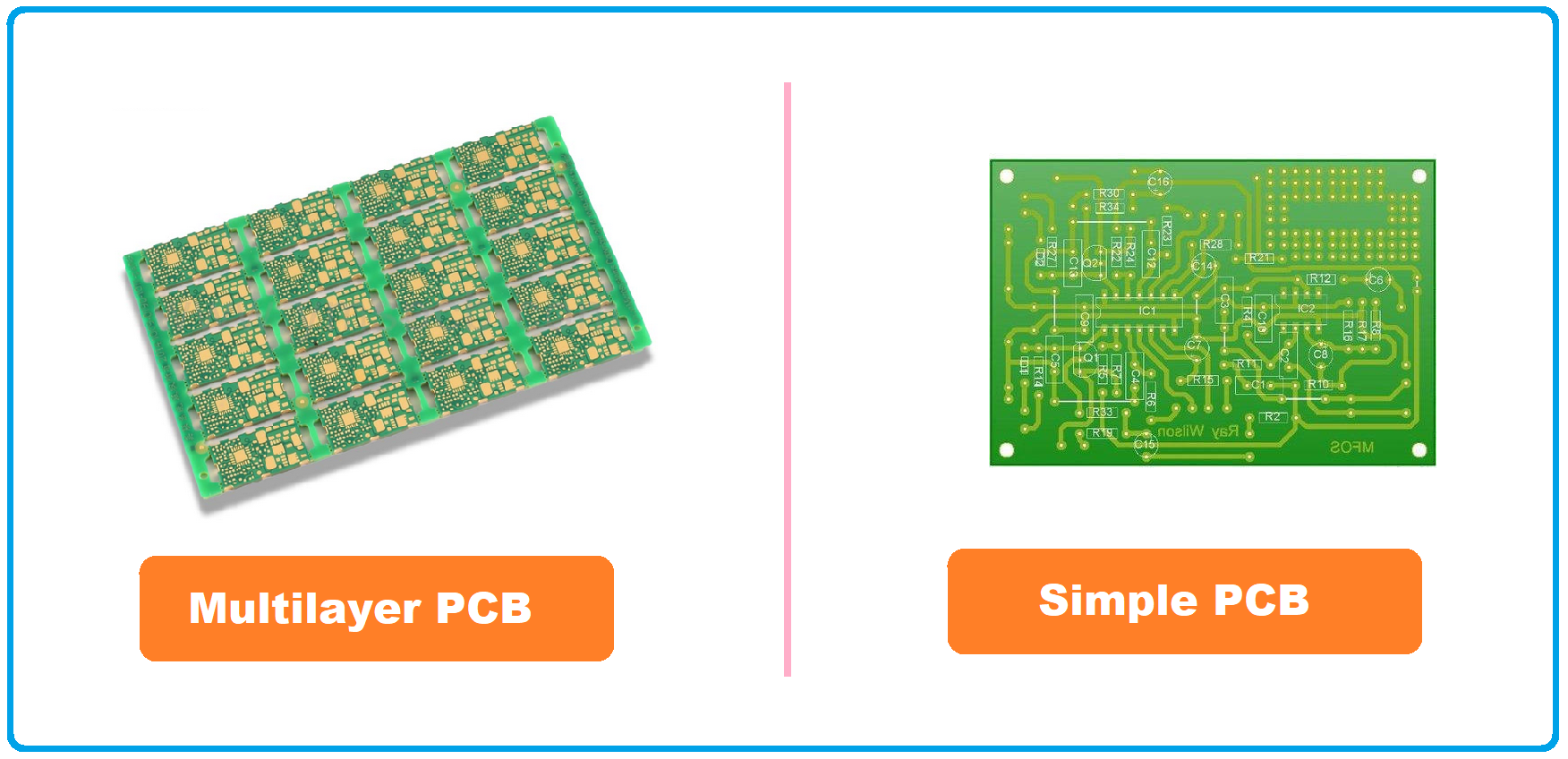
- A PCB is called Multilayer PCB if it has 3 or more layers(sheets) of copper foil, insulated from each other(by lamination or coating) and joined together to form a single piece.
- A Multilayer PCB has an Inner Layer Core present at the center of all the layers and coated with a Copper layer from both sides, while layers of prepreg(woven glass cloth with epoxy resin) are used for insulation.
- In Multilayer PCB, outer layers(top & bottom) are single-sided PCBs, while the inner layers are double-sided PCBs.
- In multiplayer PCBs, few layers might be assigned with fixed tasks and are termed as planes i.e. power planes, ground planes.
Discussions
Become a Hackaday.io Member
Create an account to leave a comment. Already have an account? Log In.