 Richie Ellingham
Tearing into Sony WH-CH510 headphones
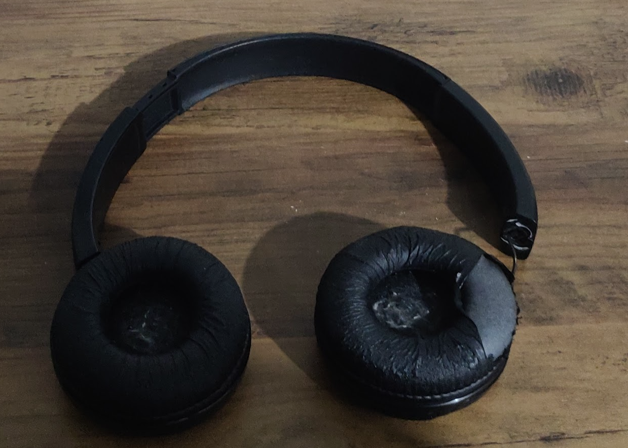
These headphones were stolen off a friend who had owned them for many years as he was going to throw them out. Why were they bin worthy? A piece of plastic snapped on one headphone, which I was able to fix with a bit of super glue. These are still in great working condition even with the thoroughly worn ear cushions.
Housing
The mechanical design of the headphones are simple the plastic curved piece of plastic has a good amount of spring to hold the headphones over a large head and could be adjusted with a sliding mechanism with multiple soft locking notches. The headphones are very lightweight so let’s open them up to see what’s inside.
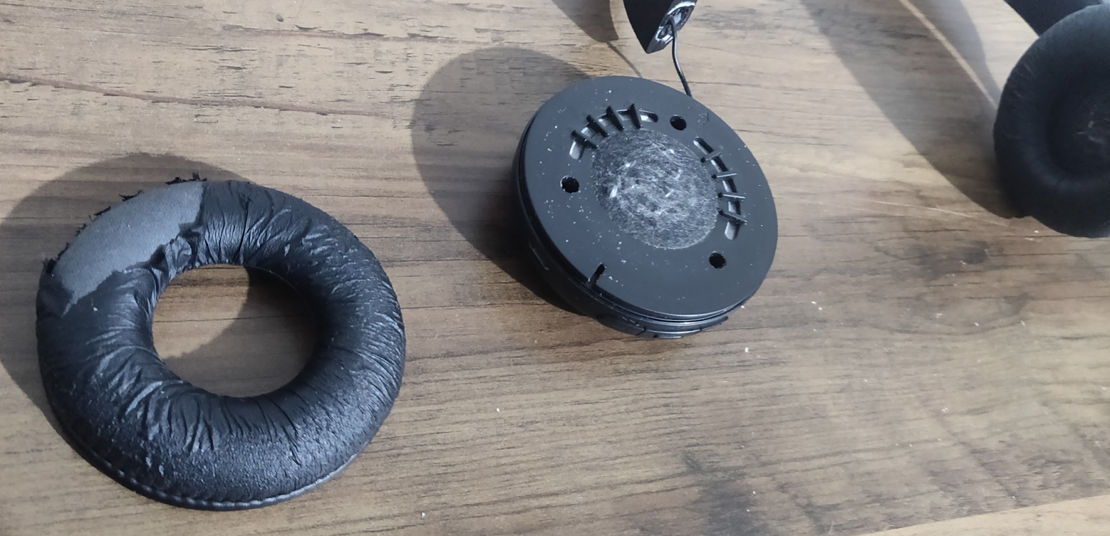
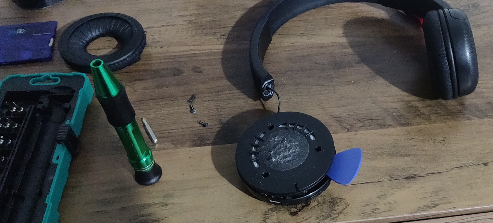
The first step is to remove the ear cushions from the headphones, which exposes three screw holes.Once the screws in these three holes have been removed you can proceed to separate this plastic plate, by levering a small flathead screwdriver into the bottom, where there is a notch in the plastic plate. Now we can see inside the headphones!
To the electron city! (aka PCB)
All of the circuitry for this device is located in the right headphone housing as seen below. This circuit is very simple and has similar components to my first teardown of some wireless earbuds. However these headphones have a much larger volume of space, sizing constraints are much less of an issue (boring!). The major components we can see when we open the housing is a 3.7 V Lipo battery, a small conical speaker and the main PCB.
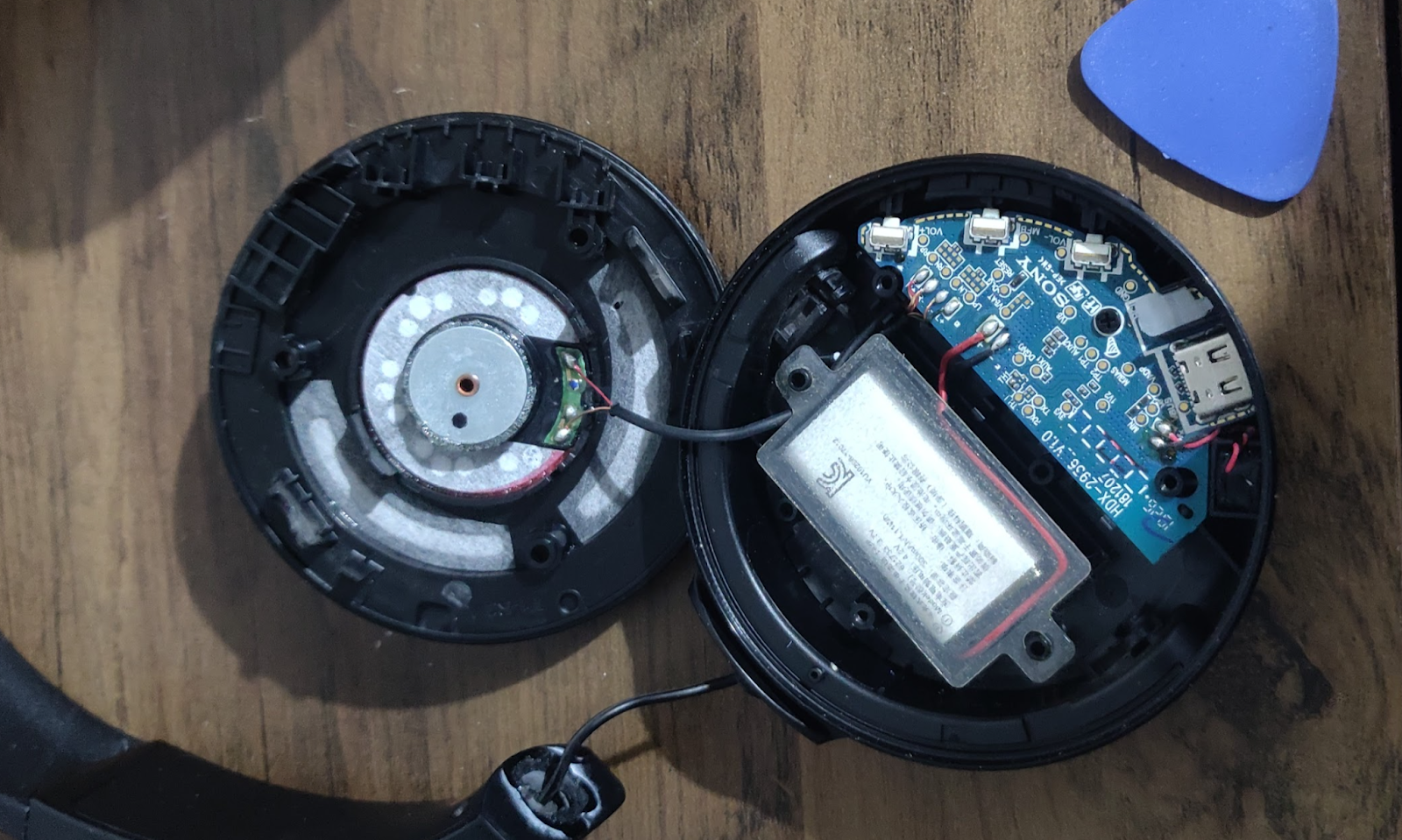
On the circumference of the PCB from left to right we have three tactile switches and LED connected to a lightpipe and a USB C charging port. The top of the PCB has very few components; only passive components like resistors, capacitors, and test points are present on this side. We call also see ‘through via’ stitching throughout the board to shield the RF parts of the circuit and ensure impedances of radio frequency lines are controlled. To reveal the other side of the PCB we simply unscrew one black screw near the centre of the PCB.
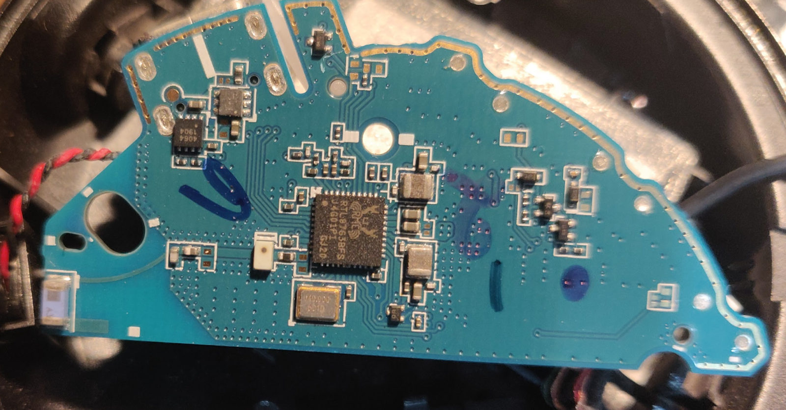
The rear of the PCB is also very simple. We have the power management circuit next to the USB header, the micro in the centre of the board and what looks like some FETs, diodes and maybe a regulator sparsely scattered around the rest of the board. The crab logo is a clear indicator that this is a Realtek SoC (RTL8763BFS). This SoC contains a silly amount of features including:
- Low power DSP - dedicated filtering microphone data and a 24bit audio codec
- Integrated dual switch mode power regulator, linear regulators, and battery charger; charging current up to 400mA
- Bluetooth radio - BLE, BT 5.0 and BDR/EDR
- USB 2.0 and USB C compatibility
- 32-bit ARM Cortex-M4F Processor
Amongst many other features somehow packed into one small package.
Below the SoC we can see a 40MHz crystal oscillator. Surrounding the SoC in close proximity are of course the decoupling/bulk capacitors.
To the left of the PCB we have an PCB trace antenna which will have all of its trace and components specifically sized to a specific impedance to optimise the radiation power of the antenna. There seems to be a blue multilayer chip antenna of sorts attached to the end of the PCB trace antenna. It is difficult to know how this antenna setup works without learning more about the intricacies of antenna engineering and the relevant electromagnetic physics principles. This is meant to be a good site for mere laymen who want to learn about antennae from fundamentals -> https://www.antenna-theory.com/ .
Conclusion
Overall a very simple teardown with proof that complex circuitry isn’t required at all when you can find a SoC that can do it all from power management to radio to processing etc. A fun quick easy teardown. They worked perfectly when put back together ready to push more well timed air pressure waves into my ears!
Discussions
Become a Hackaday.io Member
Create an account to leave a comment. Already have an account? Log In.