I recently posted some pictures of a PCB with text in pads describing their purpose (for example "5V", "GND" or "A9"):
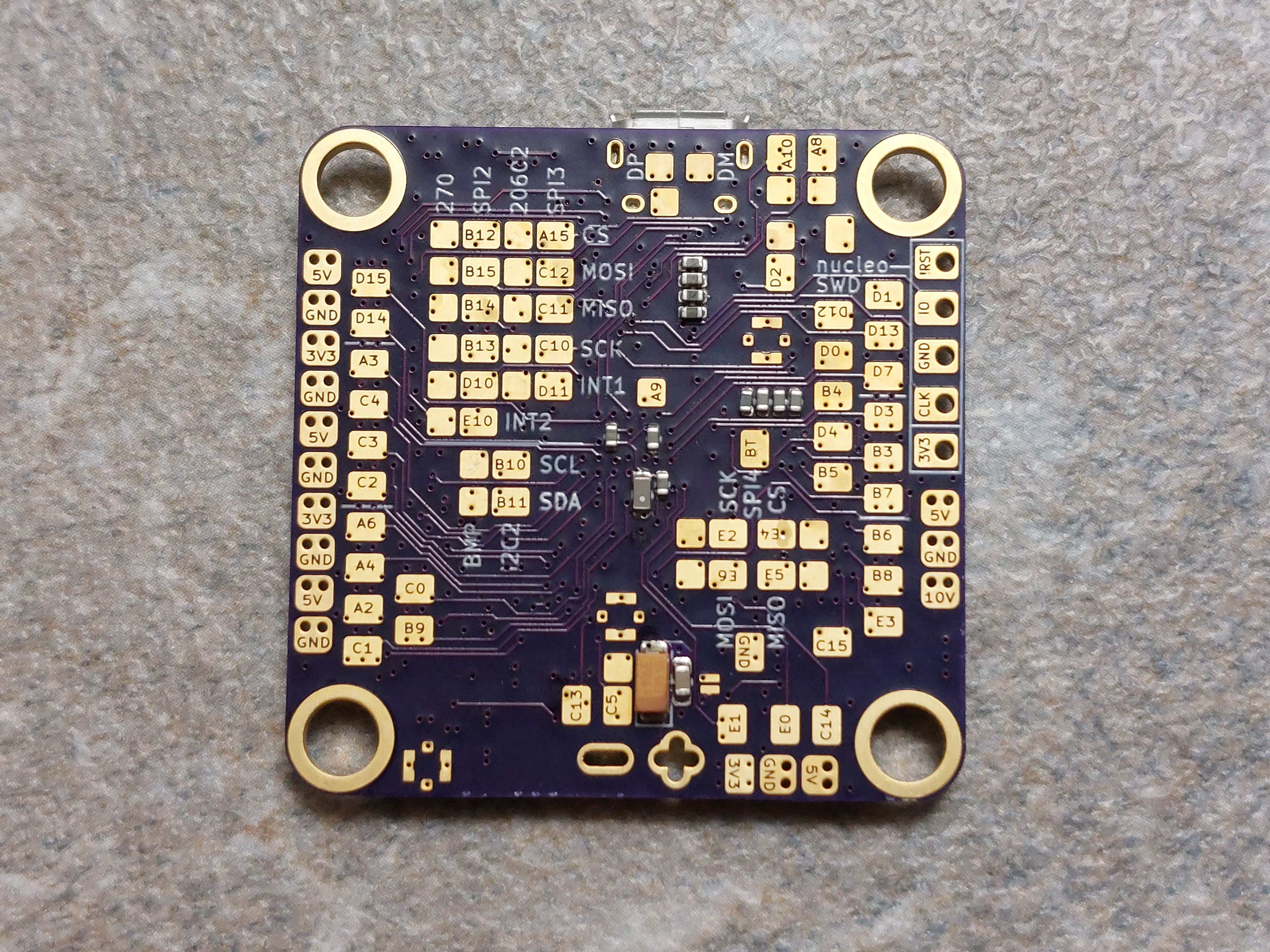
And I received lots of questions about the process, so here's a little tutorial.
A quick overview:
- Some preliminary remarks
- Prepare the layout
- Produce raw gerber files
- Subtract text from copper using gerber_combine
- Check
- Enjoy
Preliminary Remarks
Of course there were some comments on this technique after I published this page. Here are the most important concerns:
- While a label-in-pad is useful for finding a pad before you solder to it, the information is invisible afterwards.
- Difficult to probe. You can touch a dead spot in a character's center and get no electrical connection
- Solder residue gets trapped between pad voids and joint
Silk screen is still the better way to label things. I'm not recommending this technique over silk screen. For eye candy in hobby projects it's probably fine.
Layout preparation
- Make sure that your pads actually allow for embedded text! That means that the pads must be large enough and that they don't have vias where the text would be. That sounds simple, but can sometimes be difficult to achieve. Don't sacrifice electrical functionality for eye candy.
- Place the labels you want in your pads on an extra layer. KiCad has user layers for this.
Example (text height: 0.5 mm; text width: 0.6 mm; line width: 0.1 mm):
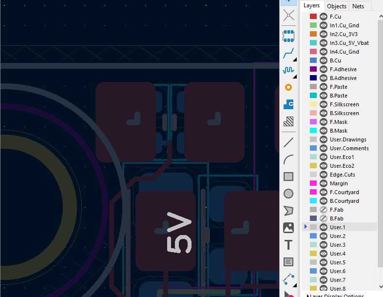
This text (or any other features you draw on that layer) will later be subtracted from the copper layer, so the end result will have better resolution than silkscreen. The silkscreen design rules don't apply here.
Producing the raw gerber files
Nothing too special, but gerber_combine requires aperture macros to be disabled. So produce your gerber files without aperture macros. KiCad plot example:
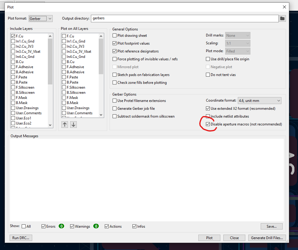
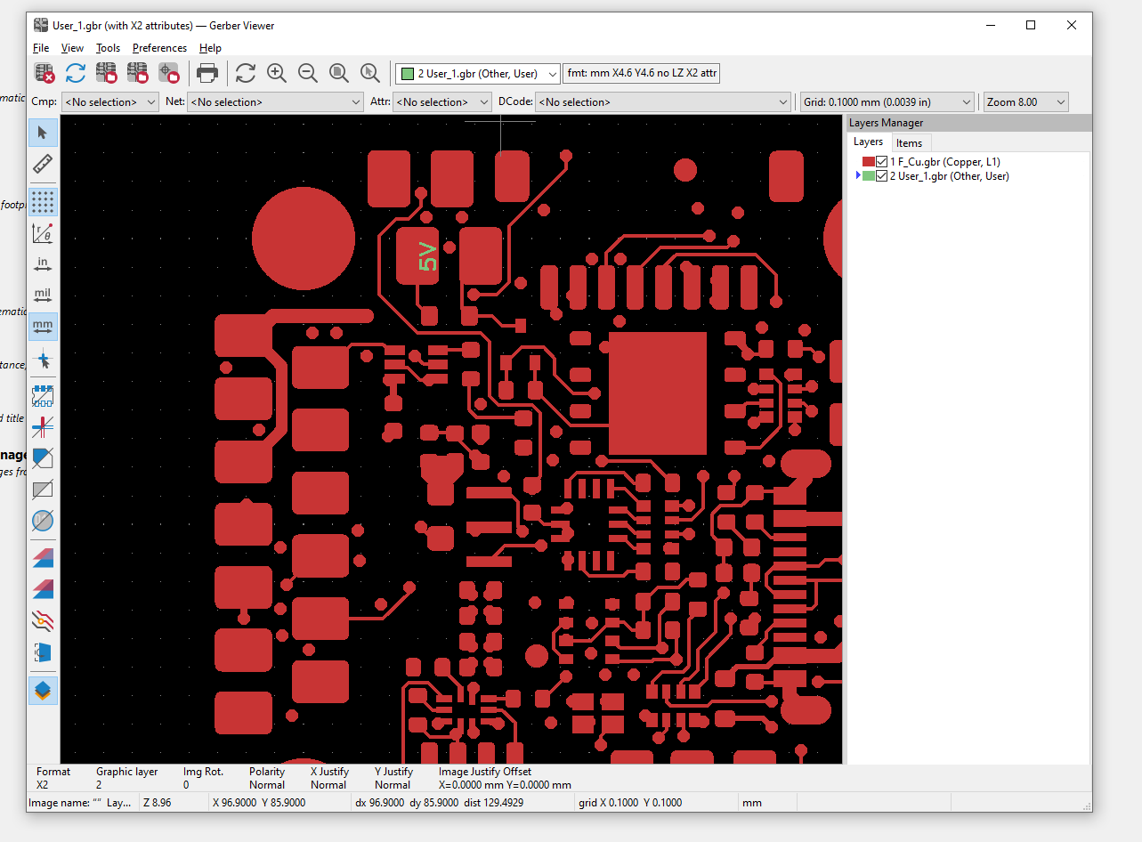
Plot copper layers and the text layers you want to subtract from those copper layers (here: F.Cu and User.1; the latter is not visible in the screenshot above). Check the raw output with a gerber viewer:
Subtract text from copper using gerber_combine
Get the gerber_combine python script from here: https://github.com/bobc/kicad-utils/tree/v5/scripts/gerber_combine and put it into the folder where your gerber files reside. Could look like this;
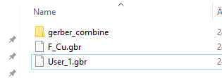
Open a terminal and enter the gerber_combine folder. Then use gerber_combine to subtract the layers from each other:
python .\gerber_combine.py -a ..\F_Cu.gbr -s ..\User_1.gbr -o ..\result.gbr
Let's have a look at the result:
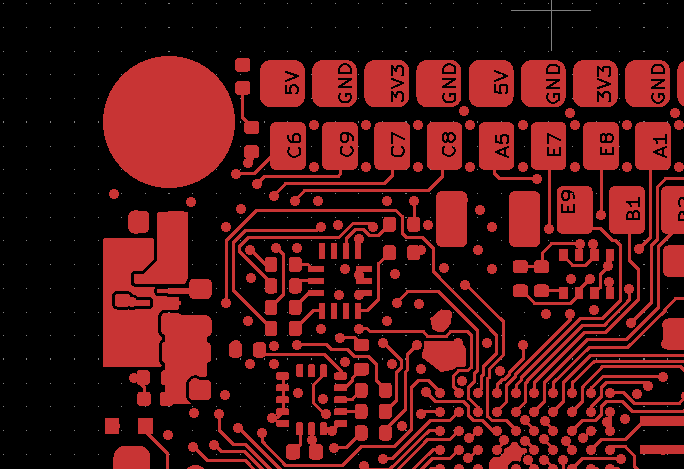
Enjoy
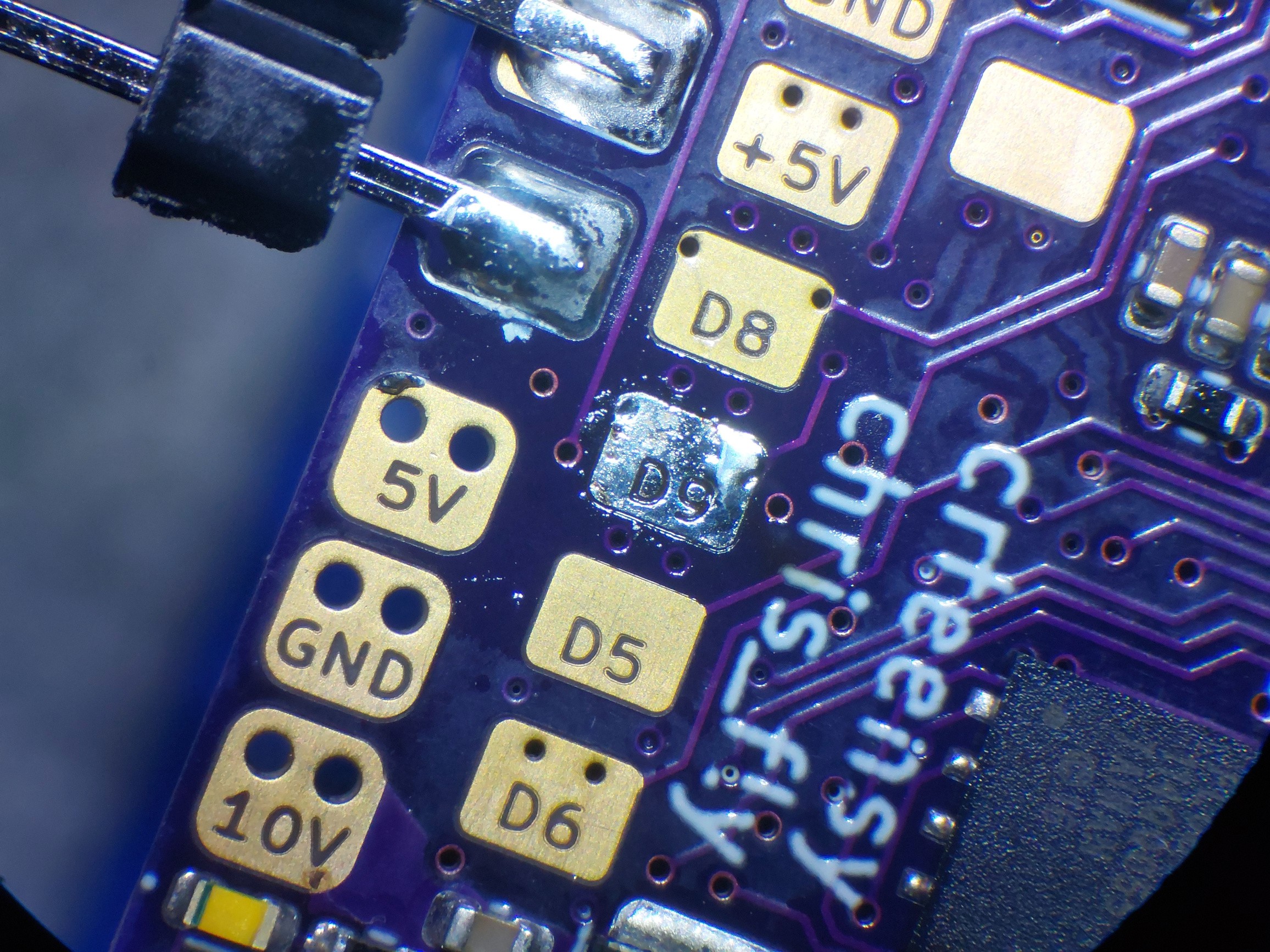
The pads still survive desoldering, just like pads that don't have text in them. Nothing has changed fundamentally:
 Christoph
Discussions
Become a Hackaday.io Member
Create an account to leave a comment. Already have an account? Log In.
VERY impressive. I love the clean look and readability.
Are you sure? yes | no
Very clever! What a great technique to add to my toolbox! Thank you for sharing! 😎👍
Are you sure? yes | no
That looks super nice!
Are you sure? yes | no
This is begging to become a plugin (or added to one).
Are you sure? yes | no