 Avi Gupta
Power electronics is a field of engineering that deals with the design and application of electronic systems for controlling and converting electric power. From renewable energy systems to electric vehicles, power electronics plays a critical role in the modern world. In this blog, we will explore the design process for power electronics, from concept to reality.
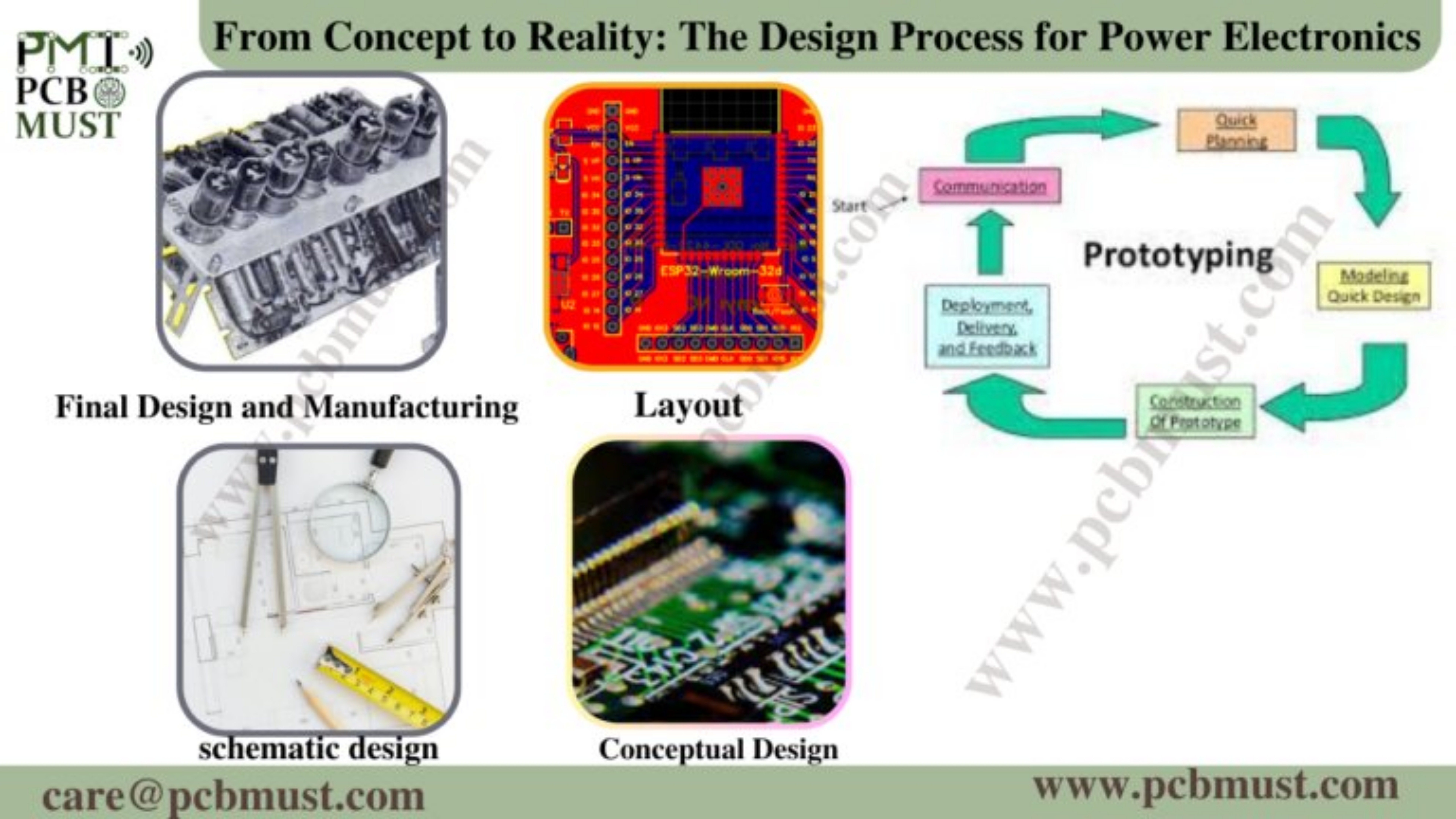
1.Conceptual Design
The first step in the design process for power electronics is the conceptual design phase. This phase involves defining the problem and identifying the requirements and constraints of the system. This includes determining the power levels, voltage and current requirements, and the environmental conditions the system will operate in.
Once the requirements are identified, the design team will begin brainstorming ideas and concepts for the system. This may involve researching and analyzing existing systems, considering different topologies and components, and evaluating the feasibility of different design options.
2.Schematic Design
Once the conceptual design is complete, the next step is to create a schematic design. This involves creating a circuit diagram that represents the components and connections of the system. The schematic design allows the design team to visualize the system and identify any potential issues or areas of improvement.
During the schematic design phase, the design team will also select the components that will be used in the system. This may include selecting transistors, diodes, capacitors, and other components based on their performance characteristics, cost, and availability.
3.PCB Layout Design
Once the schematic design is complete, the next step is to create the PCB layout design. This involves designing the physical layout of the components on the printed circuit board (PCB). The PCB layout is critical for ensuring the system functions correctly and efficiently.
During the PCB layout design phase, the design team will consider factors such as the size of the PCB, the spacing between components, and the routing of the circuit traces. The goal is to create a layout that maximizes performance, minimizes noise and interference, and is easy to manufacture.
4.Prototype Development
Once the PCB layout design is complete, the next step is to develop a prototype of the system. This involves assembling the components onto the PCB and testing the system to ensure it functions correctly.
During the prototype development phase, the design team will typically conduct a range of tests to evaluate the system’s performance. This may include testing the system under different load conditions, testing for efficiency, and testing for any potential issues or errors.
5.Final Design and Manufacturing
Once the prototype has been tested and any issues have been addressed, the final design can be completed. This involves making any necessary changes or modifications to the design based on the results of the testing.
Once the final design is complete, the system can be manufactured. This typically involves sourcing the components and assembling the PCBs, followed by final testing and quality control.
6.Conclusion
The design process for power electronics involves a range of steps, from conceptual design to final manufacturing. Each step is critical for ensuring the system functions correctly and efficiently. By following a rigorous design process, designers can create power electronics systems that meet the requirements and constraints of the application, while also maximizing performance and efficiency.
About the Author:
Avi Gupta, Founder of PCB Must Innovations, is a dynamic force in the world of electronics design. With a wealth of industry experience, Avi thrives on solving intricate problems and delivering dependable solutions. A tech enthusiast, Avi stays ahead of trends while cherishing precious moments with family.
Avi could be reached at care@pcbmust.com
Discussions
Become a Hackaday.io Member
Create an account to leave a comment. Already have an account? Log In.