 Yann Guidon / YGDES
My first 2 orders were to DirtyPCBs and were satisfying.
The 3rd was to Dangerous Prototypes because DirtyPCBs was down.
Both provide my required characteristics at very good prices : 0.6mm FR4, plated through holes, white mask, HASL finish. You'd think I'd get the same result, since they used the same factories, but I was surprised.
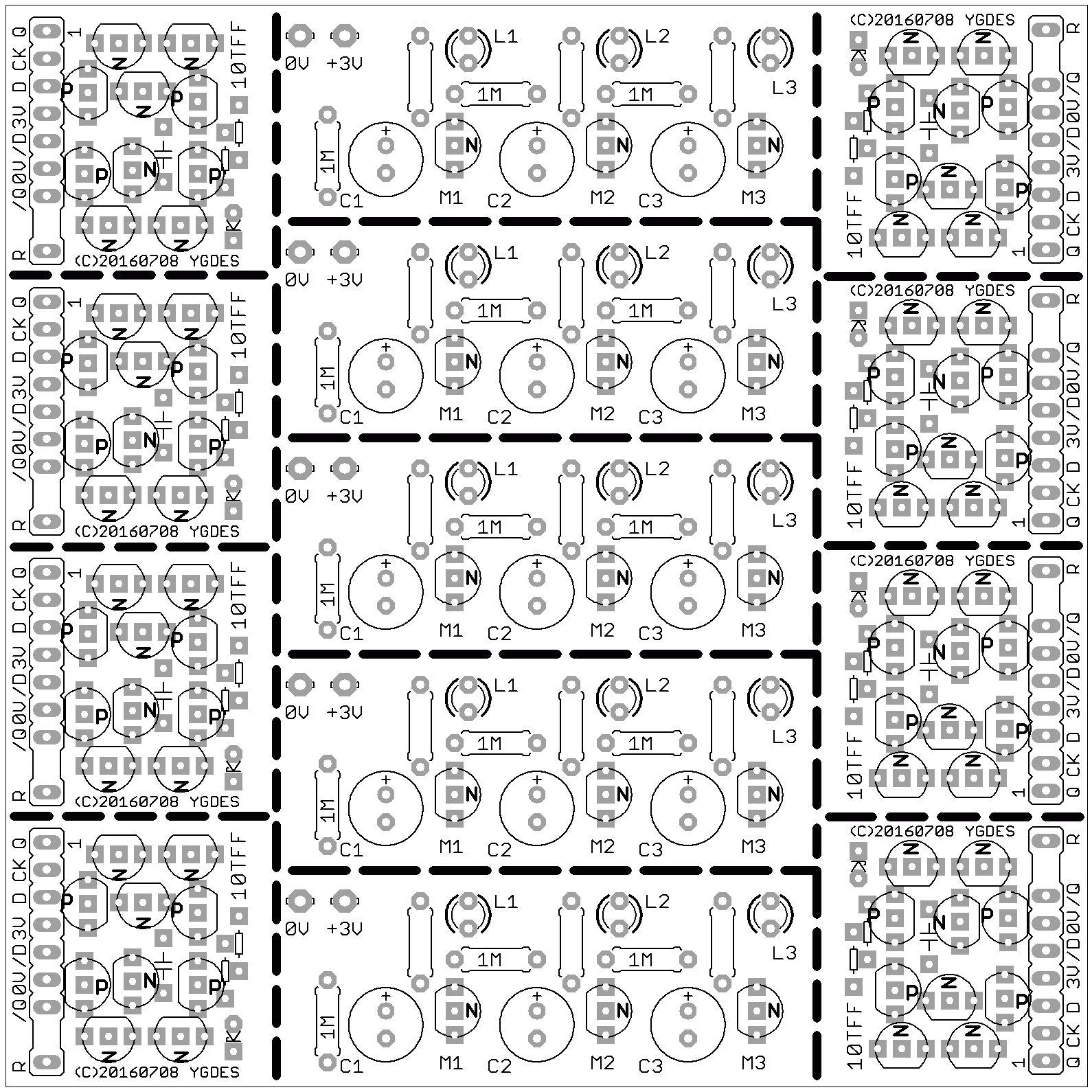
- First remark : DirtyPCB respected my milling to the letter. That was pretty cool :-) I gorget which diameter I asked (0.8mm ?) but it went well.
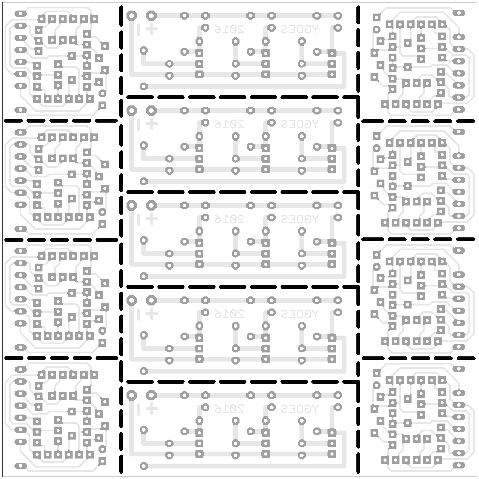
OTOH Dangerous Prototypes replaced my dashed milling to make a "classic milling" just as a normal panelized design. Pretty neat ! However I carefully selected the milling diameter because some boards have very tight dimensional margins. My caliper says around 0.8mm while I asked for 0.7mm. I'll see if it changes anything in practice... - Second remark : Dangerous Prototypes provides only a very low-resolution preview. DirtyPCBs provides high-resolution renderings that helped me get the first boards "right" at the first order.
This matters a lot because (even though the previews are not binding) the markings are important for my display projects. And Dangerous Prototypes cluttered my PCB with the very badly autoplaced parts numbers. With fine pitch SMDs, it creates a mess.
Just have a look at these previews, generated in a second by DirtyPCBs before you commit/pay:
You can easily spot issues.
Now try this on this 150×150px thumbnail:
No higher resolution is provided...
- Third remark : In the same vein, I have chosen to cover the vias with mask to reduce visual clutter and reduce chances of shorts. Dangerous Prototypes ignored my DRC (well, not their fault, I didn't provide, but they didn't ask either) and my PCB "visible side" is sparkling with all the HASL vias.
Solution to 2) and 3) : provide GERBER files. This must be evaluated...
- 4th remark : Now, a pretty miffing discovery : Dangerous Prototypes placed a PCB reference number on the visible side of one of the panelised circuits. Half of my first #DYPLED boards now have an irrelevant string. Why put it on this side ? I should "reverse" the circuit so the markings can be located on the other side....
Let me state (again?) that there is nothing "wrong" with what Dangerous Prototypes did. It's just that the result is not "as I expected". Dangerous Prototypes might have manual intervention, or maybe it was processed and checked by a different operator but nothing was modified on both DirtyPCBs runs. This (and the good resolution of the preview) is why I favor them.
OTOH Dangerous Prototypes provides more options (flex for the win !)
Overall, I have tested the process and got fast delivery for a very reasonable price and I can prototype #DYPLED and others. 0.6mm FR4 is nice, no need to use finer boards. And I know how to make the PCB I want :-)
The following pictures show the actual circuits:
- Here we see the different style of milling, and the mess generated by points 2) and 3). The user markings are unreadable.
The #DYPLED circuit is way more sophisticated than the #Yet Another Electronic Lampyridae so I shouldn't be surprised that there are more opportunities to mess something up... That's what prototypes are for.
- The issues with the mask and silkscreen:
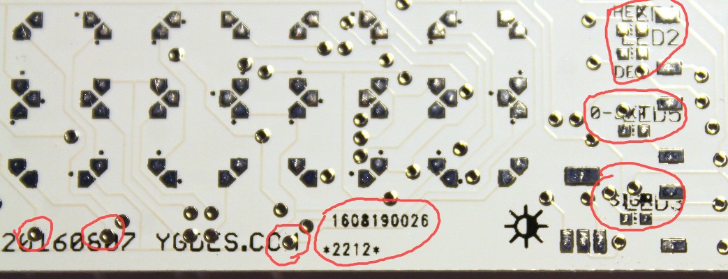
The vias are exposed, they mess with markings and will short signals, the parts references are printed and confuse the user markings, and a random, unwanted reference number is added...
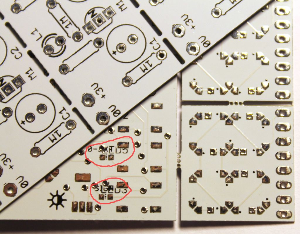
- The circuits are actually automatically tested, as can be seen by the tiny dots (from the probes) on many pads. And the process works nicely with 250µ wide pads. Look at the following picture in high resolution:
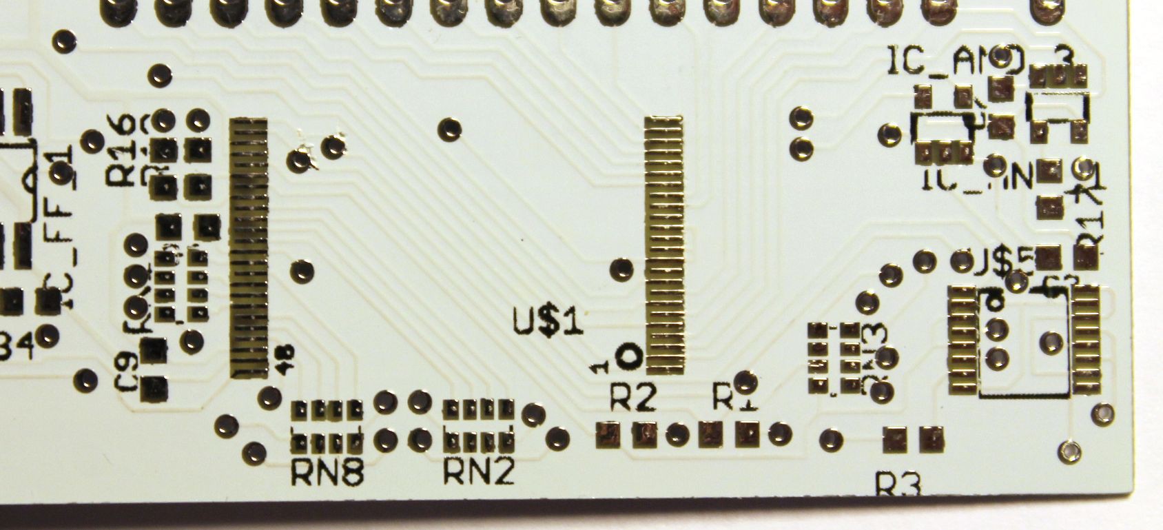
#DYPLED can move forward but the tinned vias are a problem because the 4014 LEDs have exposed thermal pads that will be shorted to other signals. Furthermore, the thickness of the tin lifts the whole LED package, which will be harder to solder... At least I can test the Flash EPROM and all the semi-discrete circuits around it.
Then I'll order a new batch wich fixes the problems I've found...
Discussions
Become a Hackaday.io Member
Create an account to leave a comment. Already have an account? Log In.
Ah hah! For some reason I went through all that and had it in my mind you used white silkscreen covering everything... Was wondering how you got it between the pads on that TSOP(?). Ahhh, white *mask,* gotcha! Looks nice.
Good lessons in here!
Are you sure? yes | no
you're welcome :-)
Are you sure? yes | no
Just a thought... Why haven't these PCB houses released .DRC file or explicit design rules ? Did I miss them ? I have shot in the dark with my 250µ pads, thinking they should be supported, with no idea if 200µ tracks were OK...
Are you sure? yes | no
DirtyPCBs has a .dru file on their about page (about 2/3 down the page). Since the specs seem to be the same between the two I used that file for my order at DP as well.
Are you sure? yes | no
Thanks !
Are you sure? yes | no
> *Be sure to check out your Gerbers before submitting them. The factory will
tell us if something is crazy, but at these prices we're not checking.*
Ahahaha that explains everything :-D DirtyPCBs for the win :-P
Are you sure? yes | no
Actually surprise that they use 0.8mm instead of 1mm bits for panelling. I have seen too many silkscreen alignment issues that I have decided to leave plenty of clearance (or omit them) for silkscreen around footprints. 24 mils and 15% ratio is my setting for silkscreen in Eagle for my Chinese PCB otherwise the lines become too thin.
Silkscreen on my solder side have been missing on my Chinese PCB. Mine also have soldermask alignment issues from time to time. I use the cheapest Chinese PCB place after all. :(
As for board designation, only seen it in my first batch and thankfully they hide it under my big PQFP. I have silkscreen names on my boards just in case.
Even gerbers aren't safe from being edited.
My share of issues: https://hackaday.io/project/4993-dual-channel-battery-chargeranalyzer/log/17291-keeping-up-with-the-times-prototyping-with-qfn-and-bga
Are you sure? yes | no
0.8mm seems to work for the milling so I'll stick to it for my next batches...
How have your GERBERs been edited ?
Yes, I saw your post while researching the issue :-)
Are you sure? yes | no
Production PCB vendors will edit gerber for things like controlled impedance tracks. They have their own DRC and scripts for improving their yield production volume. You have to ask them for the actual mask files if you want to know what's being shipped inside your multilayer boards.
Are you sure? yes | no
Yann, I share your pain on this! I have experienced these exact issues (with different vendors), especially for projects in which the board was part of a front panel or otherwise visible. It's very frustrating. To get around it, I:
1) always send gerbers (you mention this above). It works well, and I can be sure they won't drop part designations on my silkscreen. There are things they could change with the gerbers, but it makes it more difficult for them to screw things up.
2) preview the gerbers before I send them out to see exactly what I will get. There are some online previewers like this one (http://mayhewlabs.com/3dpcb). I also wrote one a few years ago (C++/OpenGL under linux) that I can put on GitHub if you're interested; it's not "finished", but works OK as is. You can check for the tented vias that are missing on your boards, and other issues. I usually catch one or two issues per board this way - even after I think it's "done".
3) "flip" the board upside down (swap all top and bottom layers) with a script (there's an Eagle ULP for this) before I send it out to keep the "identifier number" they add on the non-facing side of the board. I have tried this half a dozen times since I thought of it, and only once did they somehow manage to put the identifier on the "face" side.
Are you sure? yes | no
Thank you Ted ! I feel vindicated :-)
For the Gerber viewers, I have a couple of Linux tools.
Are you sure? yes | no