 zakqwy
I picked up a Pi Zero the other day and haven't done much with it. I should have gotten the kit, since I don't have an extra uSD card lying around and I sure as heck don't have any mini-HDMI cables. Ah well.
 [photo from Adafruit]
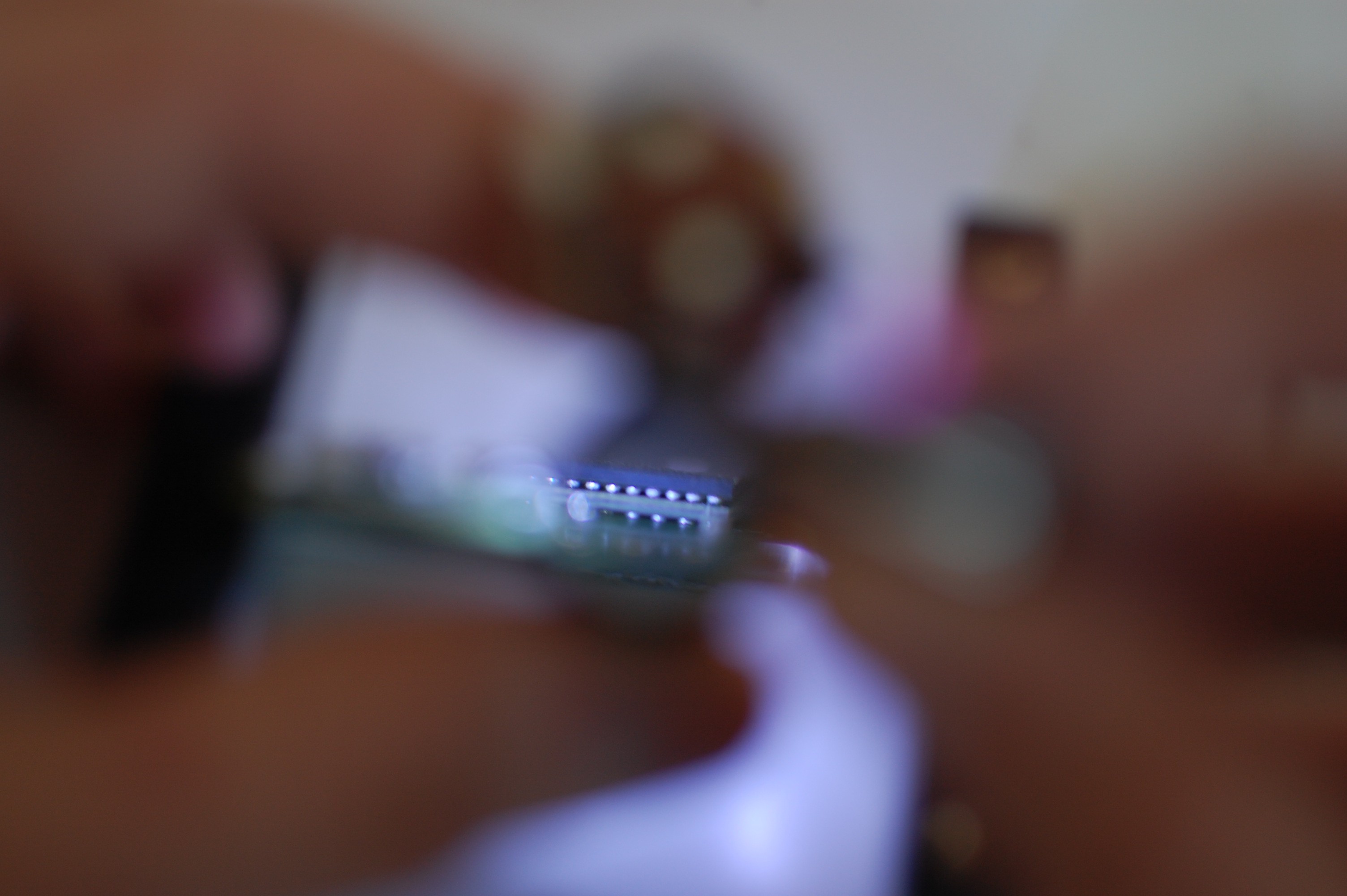
It's a pretty nifty board, as ten billion people (give or take) have already said at this point. As I sometimes do with circuit boards when I need to procrastinate, I grabbed my loupe and gave it a close examination. A few interesting items popped out which I've attempted to image below using an exceedingly crappy 'macro' setup (F1.8/D40, 10x loupe, remote shutter release, steady hands).
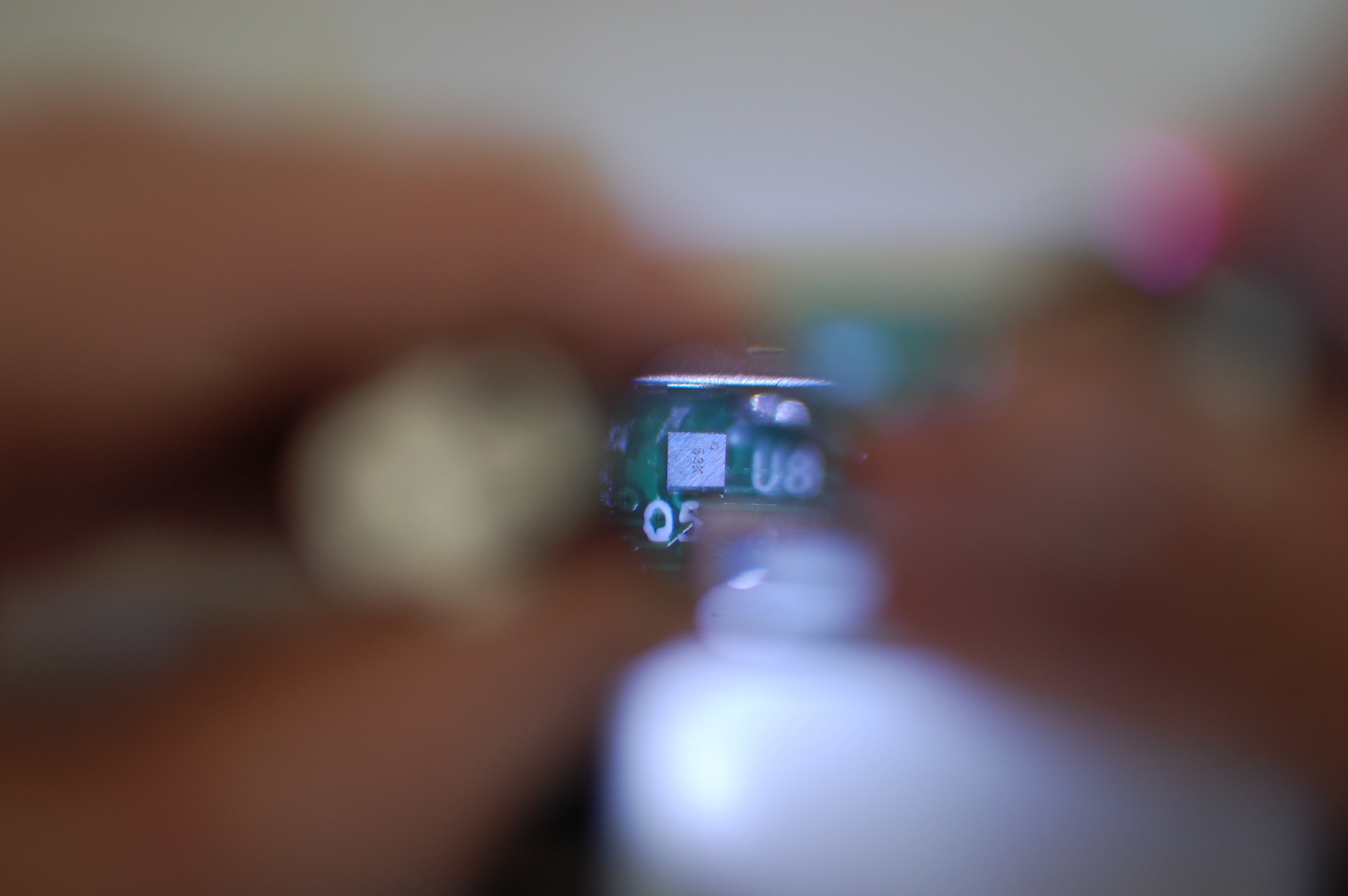
The picture above shows a close-up of the mysterious(ish) Broadcom BCM2835 SOC that runs the whole board. What was most interesting to me here is the double-stack BGA arrangement; from what I can tell, the BCM2835 rides on an FR4 plate that pretty much changes the ball pitch from ~0.4mm (guess) to ~0.65mm (another guess), presumably adding an extra row or two to make up for the decreased density or perhaps dropping a bunch of connections entirely. My theory -- the high ball density of the SOC requires a higher layer count PCB for proper escape routing, so the in-between plate allows them to use the chip with a cheaper 4 layer PCB. Anyone ever seen this before that could confirm this suspicion?
Discussions
Become a Hackaday.io Member
Create an account to leave a comment. Already have an account? Log In.
Thanks for the comments, all. While @esot.eric's photo from the RPi website is neat, now I'm dying to see the bare RAM die that's presumably on the other side. I might have to fire up the hot air station for this one and make a $5 sacrifice to the SBC gods.
Are you sure? yes | no
don't forget to document and photograph all the steps ;-)
Are you sure? yes | no
Always! I'm thinking about picking up a decent video camera, actually. Maybe tearing into the RPi Zero is a good first clip.
Are you sure? yes | no
Cool!
Are you sure? yes | no
its call package on package design and its not uncommon for highly integrated system on a chip devices.
Are you sure? yes | no
https://en.wikipedia.org/wiki/Package_on_package
thanks, that is fascinating!
Are you sure? yes | no
Another photo with a loupe : https://hackaday.io/project/13409/log/50862-inside-the-mesa-can
The flip-chip is certainly a protection diode array.
Are you sure? yes | no
your loupe pictures are superior to mine. How old are those Ge transistors? Are you looking at 50-year-old bond wires??
Are you sure? yes | no
I did work hard on this picture, it was not easy, a lot of hacking :-D
I have not found any date code, only serial numbers but this design seems to date from the mid-to-end of the 60s, 50 years ago. Some boxes are pretty dusty and the plastic is sometimes cracking. Maybe a batch from the early 70s, when the mesa process was yielding enough and prices could fall, before the newer epitaxial processes took over.
I'm not sure it's Au or Al, the wire is really toooooo thin.
I'll have to make a ring oscillator to see how fast it can run !
Are you sure? yes | no
That double-stack caught my attention, too. As I recall, the actual chip atop the board that's visible is actually the RAM, and the processor itself is sandwitched between the RAM and the PCB. Weird, eh?
'Spose a heatgun should be taken to it!
[Edit] Ah hah, here it is, too bad we can't see both sides...
https://www.raspberrypi.org/blog/libraries-codecs-oss/
Are you sure? yes | no
Clever idea with the photographing via loupe!
Are you sure? yes | no
Thanks for the photo, it's pretty neat they documented that. I was wondering where the RAM was, I guess that makes sense. Such technology, wow
Are you sure? yes | no
That is really interesting with the double stack. My guess would be that they drop pins and enlarge the pads so that they can get away using a cheaper board house with poorer DRC
Are you sure? yes | no