 Pavel
Pavel Having obtained 50 MHz analogue single channel oscilloscope opened new avenues for researching of electronics. Here I will present the results regarding measurements of logic gate parameters.
I started with the most basic "gate", made up from one diode and one resistor. This is diode logic gate AND with only one input, something like buffer. Here is the schematics:
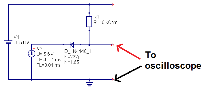
As I looked at slope of the rising edge, it became apparent, that it is depended on the value of resistor used. The less resistance, the more steep edge ensures (following are my drawings from oscilloscope screen; 1n60p is Schottky diode):
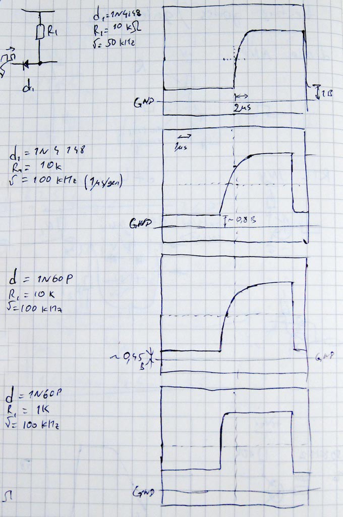
This circuit is used as input stage in my gates, so getting fast response from it is essential. On the other hand, it is curious for me, as I had read that diode has very little capacitance and can switch to and from conduction in matter of picoseconds. Somehow it seems that it does so only when switching from noncunduction to conduction. For it to stop conducting it needs some time, as though there is a need for some charge to be pumped? The more current flows through it, the more readily it ceases to conduct, it seems. By the way, using Shottky diode instead of regular one made no apparent change.
Anyway, proceeding to proper gate, the DTL inverter:
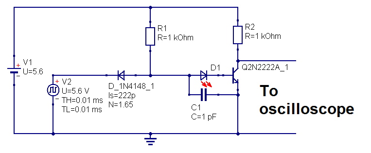
The schematic shows the one I came up with, which is the best for its speed (has delay somewhere near 175 ns).
Here is account regarding search for right combination of resistances and capacitance:
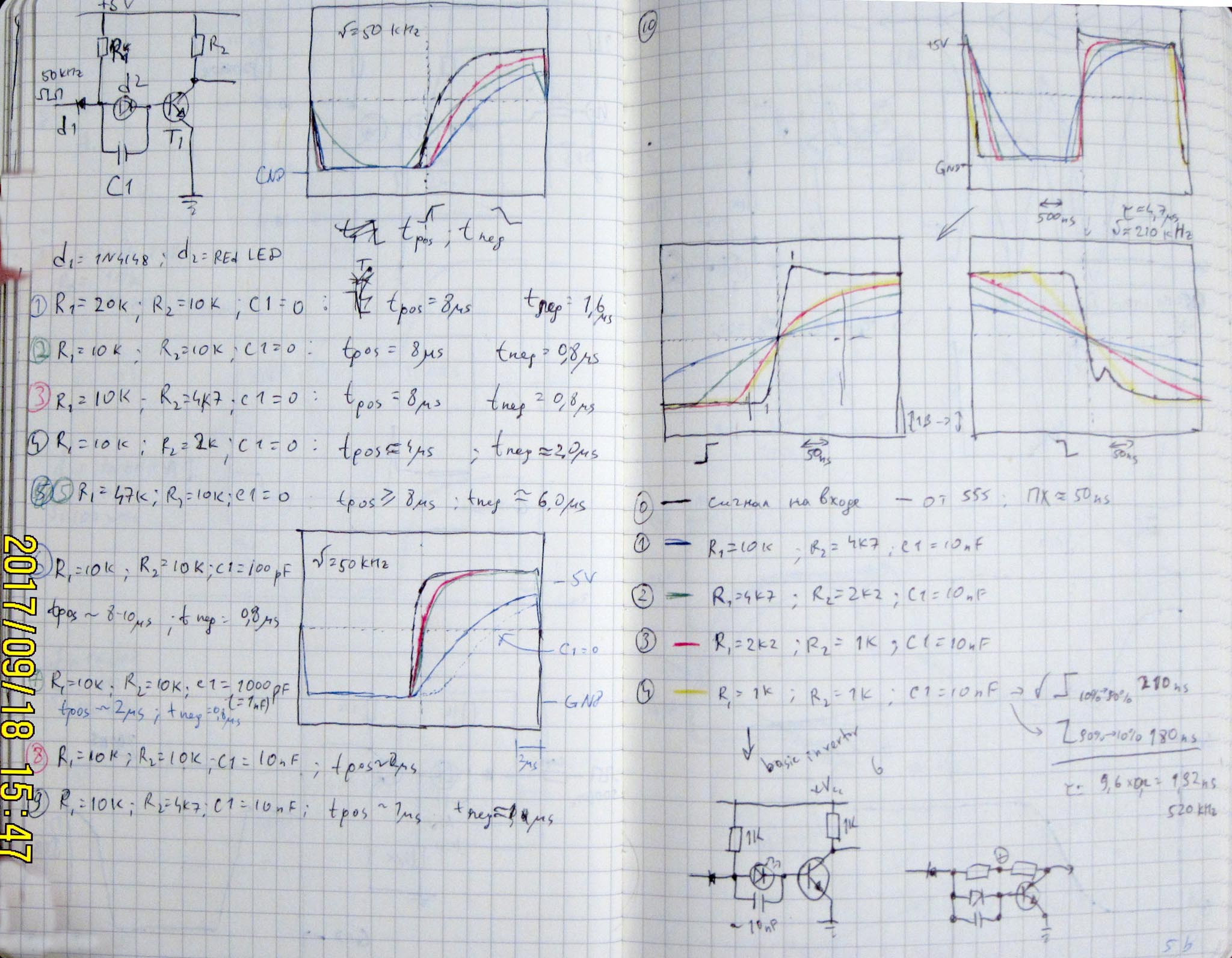
Square wave signal of nearly 50 kHz is generated by 555 IC, it have nice edges with rise and fall times less that 50 nanoseconds. On graphs on the right page it represented by solid black line. As one can see, adding capacitor makes for much faster response of transistor -- it switches off much faster. Also lowering resistor values makes for sharper edges in general (lowering R1 makes falling edge sharper, and lowering R2 makes rising edge sharper).
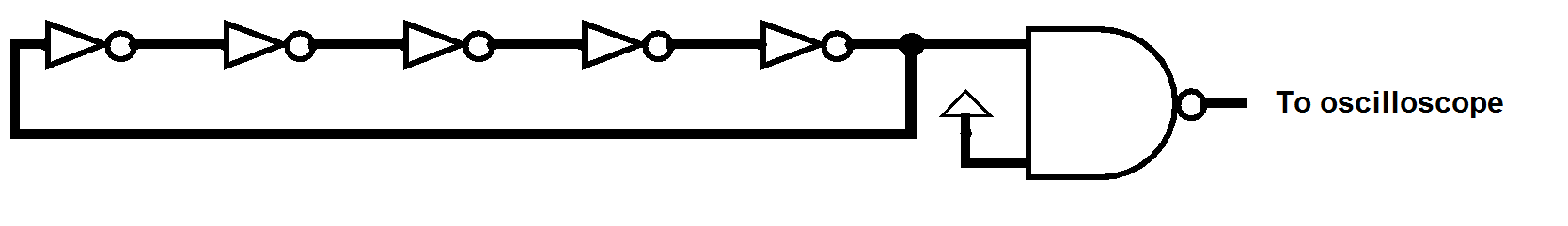
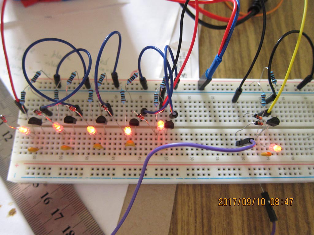
For measuring gate delay I used chain of 5 inverters with output from 5th fed to input of first one. From there also tapped signal to oscilloscope. That way I had free oscillations with period = 10*delay time.
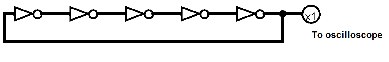
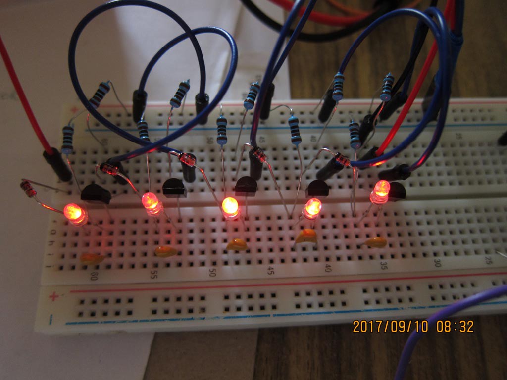
Here is the picture of such setup:
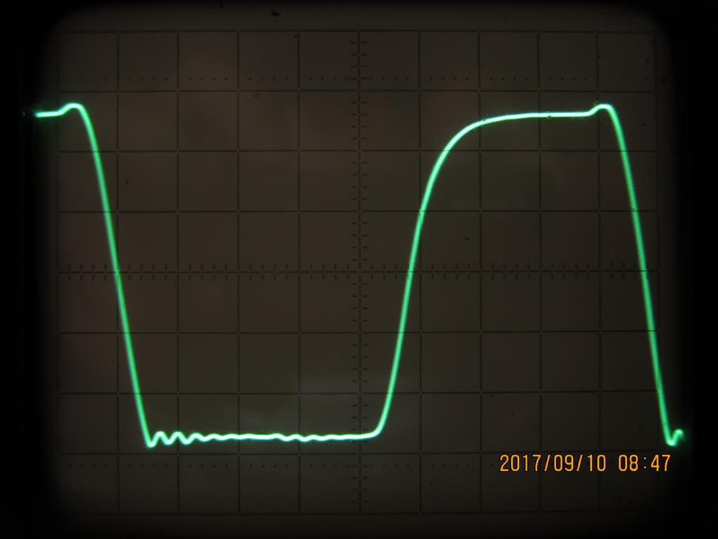
And this is the trace on oscilloscope screen (reticule: one cell horizontally = 200ns, verically = 1 Volt):
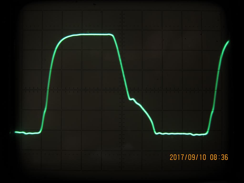
As one can see, falling edge of output from gate, when loaded by the next gate becomes slower after it falls below certain level (1.95 V above ground) which coincides by LED's drop. Why is it so? When gate is not loaded, or loaded by simple resistance to ground, the falling edge is featureless:
By the way, adding resistor from base of transistor to ground have not yielded good result -- while it makes rising edge slightly sharper, the falling edge quite noticeably becomes less sharp.
Also I tried to use capacitors in parallel to input diodes, and another time replaced input diode with transistor -- while there was some improvement in delay time (it became as little as 125 ns) and I was able to use higher resistance at input, there was drawback, in my opinion: while gate was loaded by another gate (like in invertor chain), HIGH signal had been lowered almost to a half value of positive rail. By the way, when measuring unloaded signal (like in the last series of pictures), output signal had full swing from rail to rail. Why? I am personally at loss here.
Discussions
Become a Hackaday.io Member
Create an account to leave a comment. Already have an account? Log In.
Welcome to the analog side of the digital world ;-)
Are you sure? yes | no