 JP
JPFor some reason boards exported from Eagle to Fusion 360 refuse to add or change decal to the model. It does not prevent to use fusion 360 as a renderer.
This short tutorial explains how to prepare textures from Eagle project and use it on the model in Fusion360. Using tips from this tutorial you can prepare model from any EDA software which let export PCB to the STEP format.
To prepare the
textures we need graphics editing tool like GIMP or Adobe.
EAGLE
First we need to prepare textures of the top and bottom side of the PCB. Separate files for: copper, silkscreen, soldermask and board outline. Exporting layers with default layer colors require additional work to do in gimp. The best way is to export layers in monochrome.
Fit board to screen (View→Zoom fit) and select top copper layers: top, via and pads.
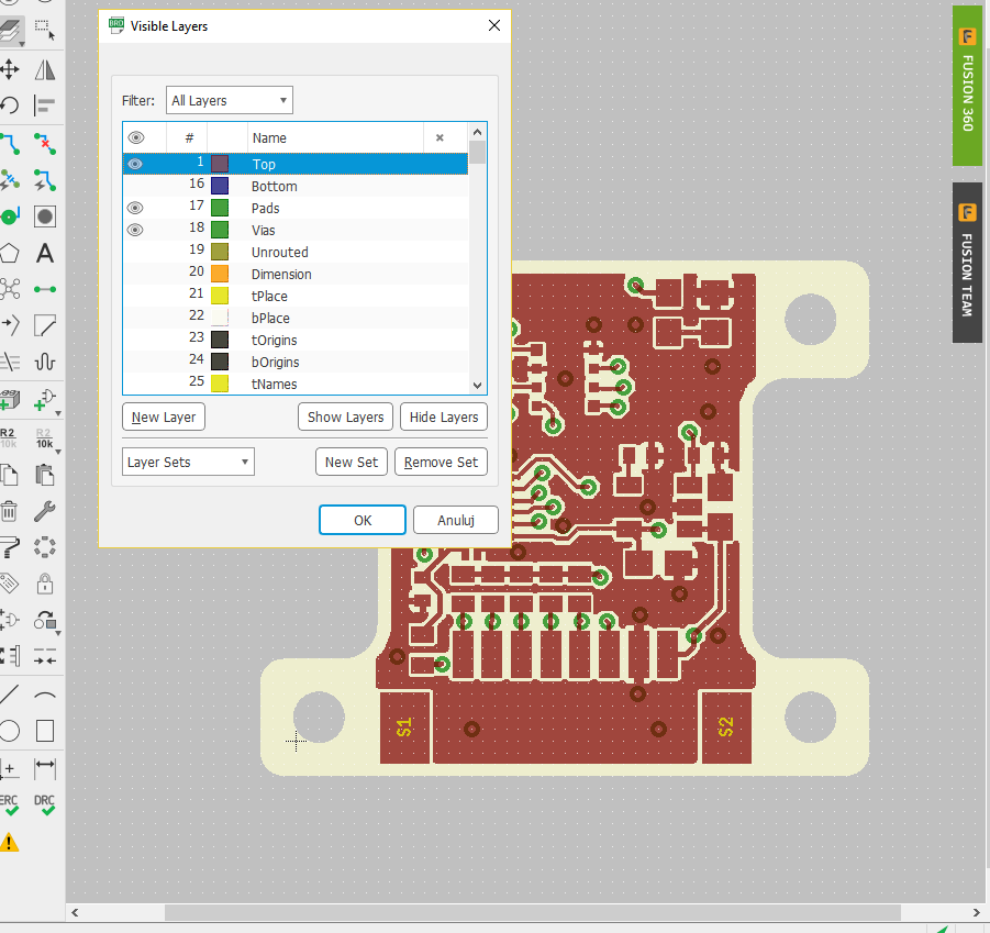
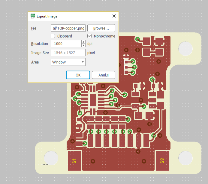
Export image (File→Export→Image) to file and select monochrome and area: window.
Select silkscreen layers: tPlace and tNames.
Export image and select monochrome and area: window.
Select soldermask layers: tStop. Remember to change layer fill to solid. This layer is needed to make pads transparent.
Export image and select monochrome and area: window.
Select outline layer and export the same way. I use outline layer to fill board with solder mask color.
GIMP
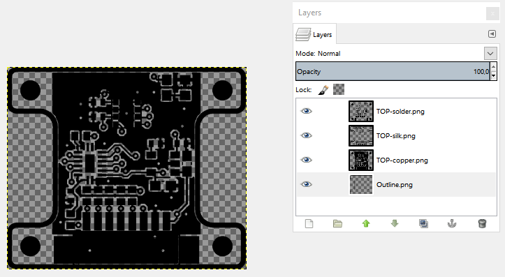
Open gimp create new file (i.e. 2000x2000px) and drag files (instead of drag and dropping files you can export to clipboard and copy past it) to the canvas. It will create new layers.
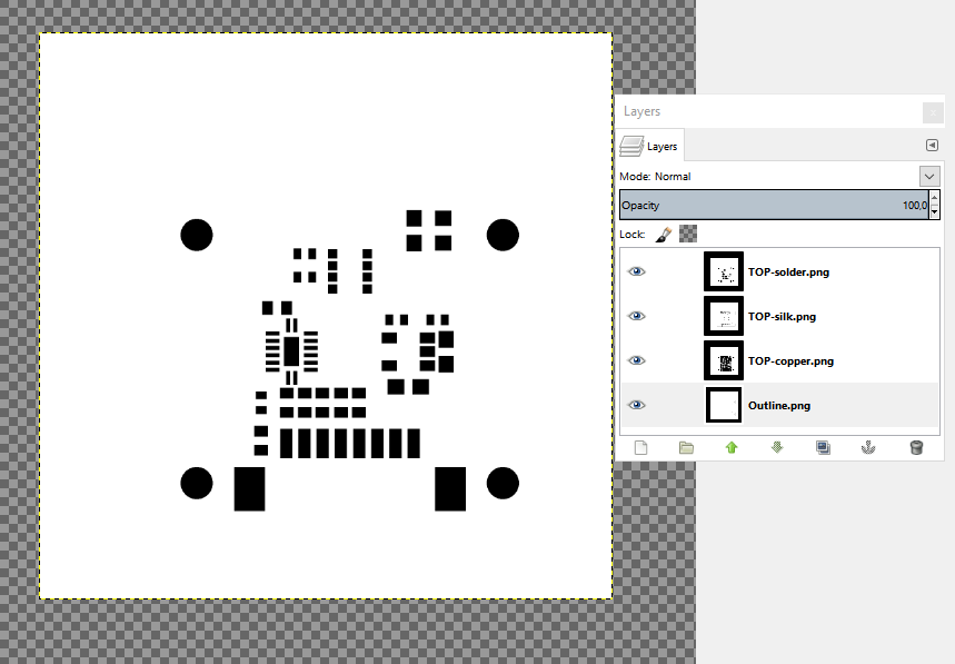
All images are on white background. For each layer remove white background using Layer→transparency→Color To alpha.
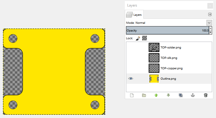
Select outline layer and crop image using Image->Autocrop image.
Hide all layers beside outline. Select desired soldermask color and fill the outline.
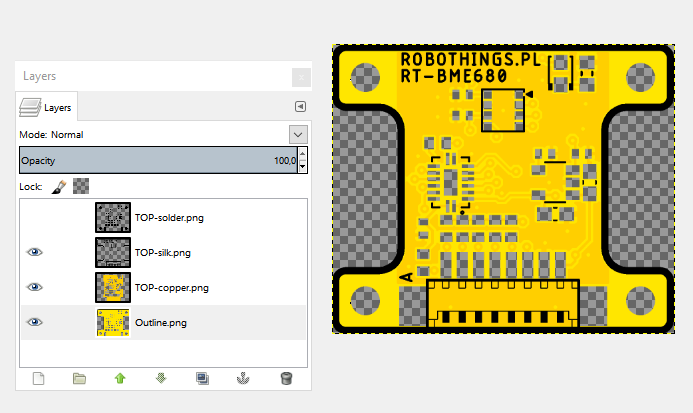
Hide current layer and unhide copper layer. Use Select by Color tool to fill selection with desired color.

Select→none.
Now it is time to reveal copper pads. Unhide soldermask layer and select all pads with Select by Color. Hide soldermask layer and use selected area to remove paint from copper and outline layers.

Last thing to do is silkscreen color change. Same as before select silkscreen with tool and fill selection with desired color.
Now texture of PCB top should looks like that.
It is ready to export. Save it to png. Repeat with PCB bottom side.
Fusion 360
This is time to run
fusion 360. I assume you already pushed project from eagle to fusion
360. Open project and use save as to export file in STEP format.
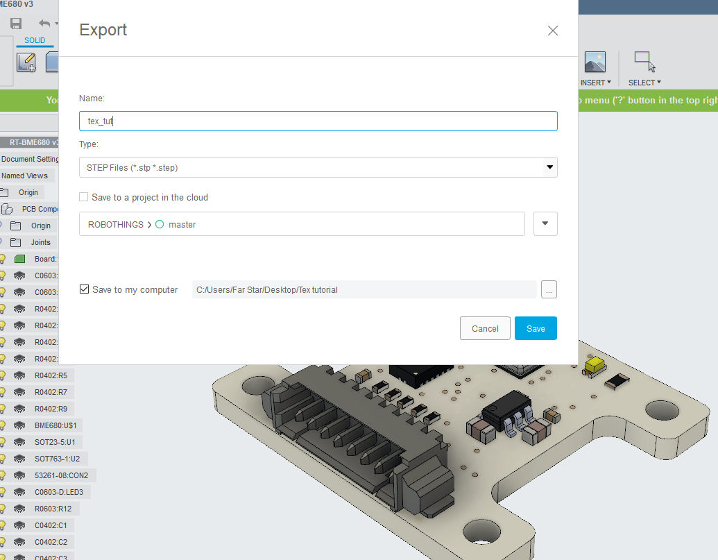
Use Open to import saved step file and to create new project.
Change workspace to render.
Select Decals tool.
Deselect Chain Faces checkbox.
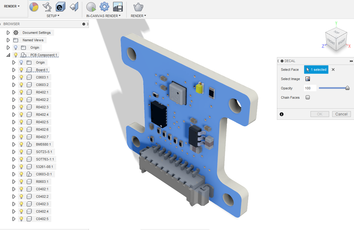
Select the PCB top face. On this surface you will put your the texture.
Select file with image.
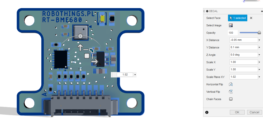
Move and scale
texture until it will perfectly match the PCB.
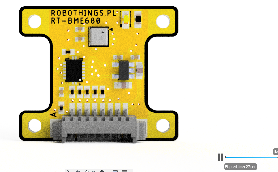
For effect of shiny metal select Appearance tool, check apply to face. Use Search form to find in the library: lead, tin or copper material. Apply it on textured face.
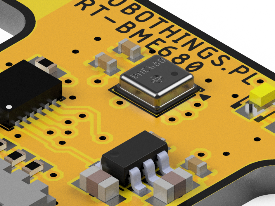
Try in-canvas render to see result.
Tutorial is quick, because I wrote it quickly.
Discussions
Become a Hackaday.io Member
Create an account to leave a comment. Already have an account? Log In.