It's Friday just before work day, so I sent it off hoping to beat the weekend.


You know it is a tiny PCB when the postage alone is easily worth $0.95. When the board is this tiny, it could easily fit into otherwise wasted space in a batch.
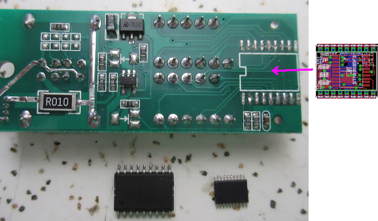
Oops. flipped the soic foot print. Have to redo more routing. This is why I procrastinate on ordering PCB. When I don't, I miss something.
This is how it would look sitting on a SOIC20 footprint. (Too lazy to make up a soic18). The pads are a bit narrower on the USB meter, but it should hold.
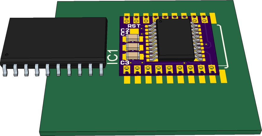
It turns out that I can make a PCB adapter that fits the STM8 to the SO18 (wide) pads. I was going to try to make a flex PCB, but decided to try out the making a Castellated Edges 0.8mm (0.031") PCB instead.
All the GPIO are broken out + 1 pad for the Reset on 0.05" pitch. The pinout is weird as it is a STM8 adapter for the SOIC-18 pin USB meter microcontroller that I have previously wired by hand.
It's going to take may be 3+ week from OSH Park.
------------------------------------------------------------------------------------
It has arrived. Original chip (SOIC-18 wide) vs tiny PCB.
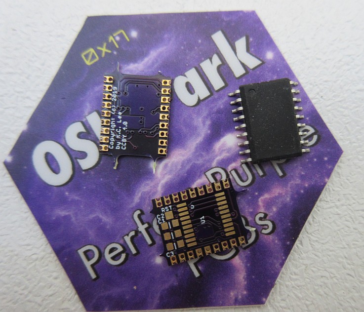
It isn't perfect, but good enough for me. Some of the barrel was removed by the milling. The hole size was 0.0197" (0.5mm) vs size of mill ~1mm.
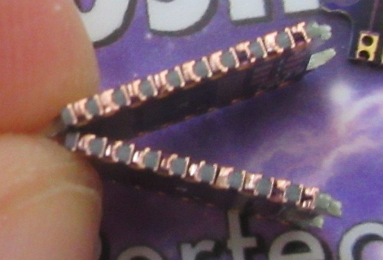
I taped down the tiny PCB for reflow. I recycled the old parts from the mod.
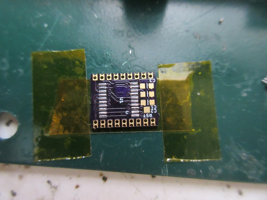
I think it works well enough. It takes a bit of extra heating to make sure that the solder seeped under the pads as well. (The 2nd pad to the left was peeled off when I did the initial mod. )

I cleaned up the mod wires. I routed Gnd, SWIM and Reset (pad RST) to the programming connector. Some of the solder wicked through the via on the inner pads.
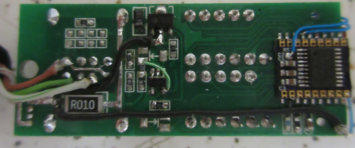
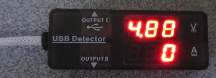
It lights up.
 K.C. Lee
Discussions
Become a Hackaday.io Member
Create an account to leave a comment. Already have an account? Log In.
Castellated edges? That's a cool idea!
Why not go for 2mm instead of 0.08" like the ESP-12? This would open a nice supply of cheap prototype boards!
Another option would be using the ESP-14 pin-out. Hmmm... interesting idea :-)
Are you sure? yes | no
Ah, please let me know when the board is available on Oshpark (if you're using KiCad and GitHub I can also do a quick review).
Are you sure? yes | no
Thanks for the offer, but I am using eagle. The new board is done. I'll send it off this morning. I'll put it up on github
https://github.com/FPGA-Computer/USB-Voltage-Current-Meter/tree/master/hardware
Are you sure? yes | no
It is an adapter board for my USB meter mod to replace the mess of magnetic wires that I was using. I have to solder it onto the existing soic18 (wide) footprint. soic = 0.05'' (1.27mm pitch). See updated picture in post.
PCB is to be soldered onto the empty footprint on right hand side. :) PCB is the size of the SOIC18 chip I pull out. I wouldn't bother with a board otherwise.
Are you sure? yes | no
Now I see my mistake: I confused "0.8mm PCB" with the pitch of the castellated terminals. 0.05" pitch is quite a feat.
I tried importing your Eagle files into KiCad, and it almost worked (there are some problems with the fill areas, the castellated vias are round, not sqaure, and the schematics have some rough spots, too. Maybe I'll clean that up and publish it in a fork of your GitHub repository.
Are you sure? yes | no
There isn't much point using this layout as the pins are scrambled for the target uC. You probably want one that is closer to the original STM8 pin out or at least grouped in a more logical order.
Castellated PCB is a first time for me, so I'll have to see how it works out. The drill holes are 0.0197" (0.5mm), so they are tiny and probably useless. I picked the 0.8mm thick PCB because of height reasons, but it would likely help a bit with the aspect ratio. The PCB probably be hot air reflowed like a leadless package.
Are you sure? yes | no