 Ken Yap
This time I sampled JLCPCB's fabrication service. This is a popular one because of their always available offer of 5 boards for 2 USD. I decided to get a panelised board made. I was assured that this wasn't a problem, but was curious.
Incidentally JLCPCB is in the same group of companies as LCSC and EasyEDA so one account will get you into all the sites. I discovered I had some introductory shipping credit at JLCPCB which meant that I only paid the fabrication charge, yay! You can also get introductory credit at LCSC. BTW it's a good official source for parts but there is a minimum order amount and shipping charges. It's also a good place to get chips not sold elsewhere, e.g. made in China chips such as LED drivers.
The usual disclaimer: This is a board with 0.1" pitch THT components so not demanding. The project is one of the first I built when returning to hobby electronics, using salvaged parts, but only on breadboard, then on perfboard. I realised that with only two ICs on board, I could fit everything in 100x50 mm and have a panel of two. Well a few mm less than 50 to allow for the break tabs.
I ran the panelizer mentioned here. One thing I had to do was rename the edge cuts file from .gm1 to .gko extension for the panelizer. This may not be necessary any more, depending on updates to the software.
JLCPCB's order page is fairly standard. Here are the instructions. I took the cheapest options which were all I needed. You also upload a Gerber package there. There is a Gerber viewer but I prefer the PCBWay open source one which you can use for free. After you have entered all the parameters and uploaded a Gerber file, you will be asked to pay, by credit card or PayPal. Then it will go through a design check by their engineers and presumably they will contact you to rectify issues before sending to production.
When the job has gone into production, there is a link to a progress page on your order page where you can see it going through the various steps. As they promised this process only took 1-2 days. However the start of the job was delayed by the onset of the Golden Week national holiday in China when businesses shut down for a few days. I didn't mind because I'm used to delayed gratification for my hobbies.
A week later, I got an email saying that my order had shipped. I had taken the cheapest postage option, registered air mail (did I already mention I'm cheap? 😀) so I was prepared for a wait. It turned out to be only about 10 days from the end of production. Caveat: I'm in Australia, it will be different for other destinations.
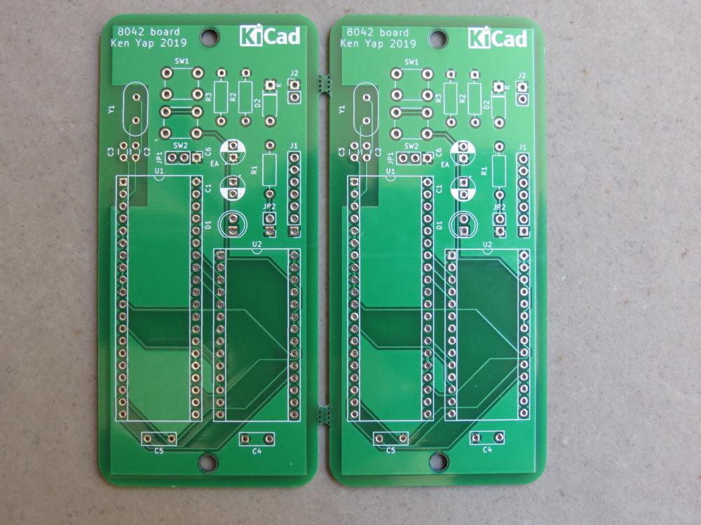
The package was a very well sealed bubble wrap one with 5 boards. So how is the quality of the boards? The front copper side:
The back copper side:
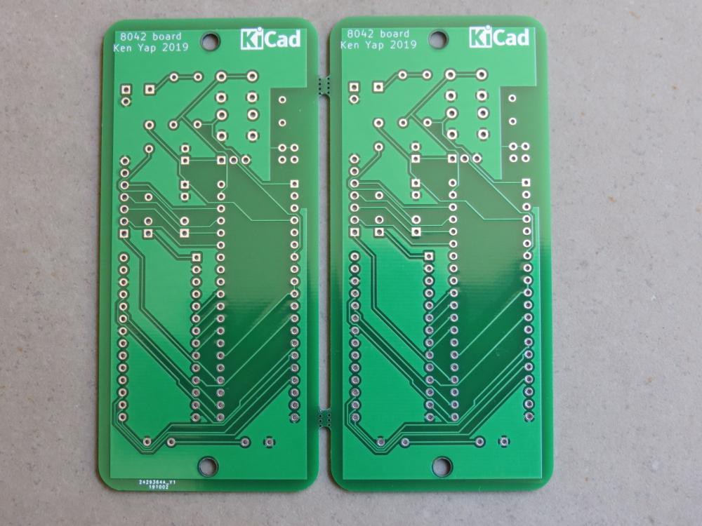
No complaints at all, all the tracks and printing were crisp. Incidentally notice the order ID they placed on the lower left hand side of the back silkscreen. You can override this order ID if you like.
So JLCPCB is one fab I will continue to use. The 2 dollar offer is for a quantity of 5 and good for prototyping when you are not sure if you will need to redo the design.
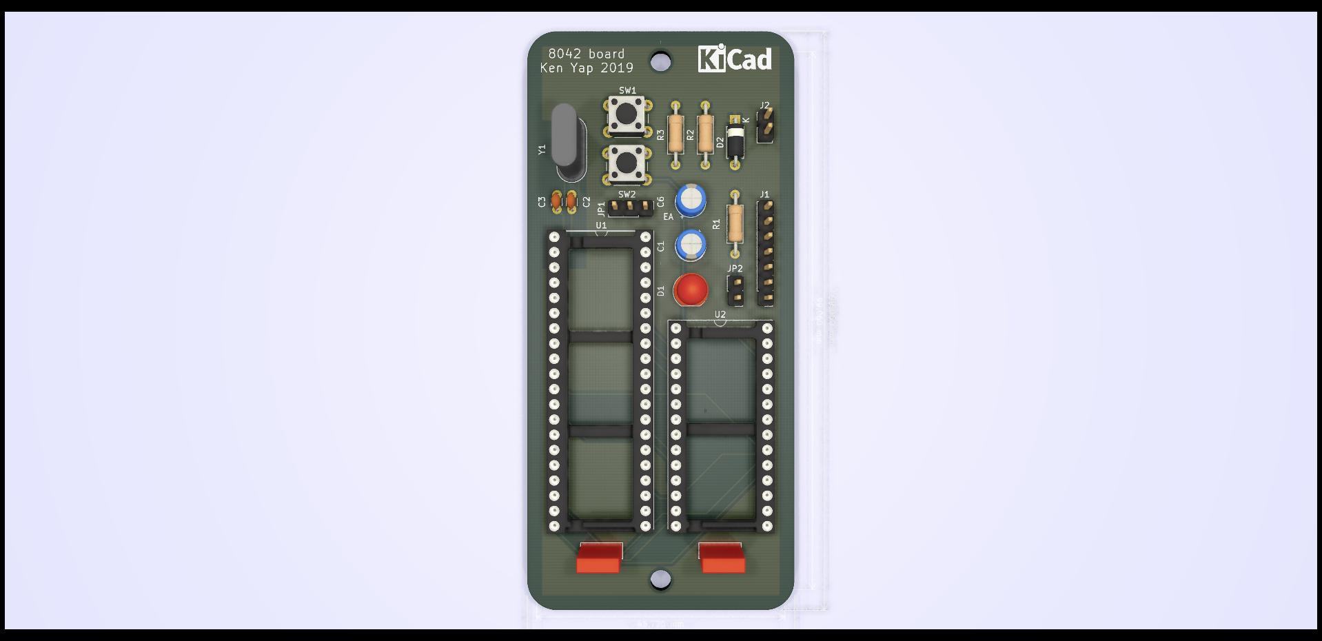
I have updated GitHub repository with the design files. This is linked to in the project. I'll update this log with another photo when I have built a board. In the meantime, enjoy this raytraced depiction of what it will look like. I used footprints for IC sockets instead of ICs.
Discussions
Become a Hackaday.io Member
Create an account to leave a comment. Already have an account? Log In.