How to generate alternate clock signals for Xilinx Artix-7 FPGA and Alchitry Au
This article started out by asking a simple question: "What if I wanted to drive my Alchitry Au FPGA design with something other than the 100Mhz master clock? " What resulted was a trip down a rabbit hole that was as distracting as it was rewarding.
If you'd like to be spared the deep-dive and get right to a concrete example, you can skip to the end for a practical introduction and come back here to understand the underpinnings of what's going on.
From the top-level documentation for the Alchitry Au FPGA, featuring the features a Xilinx XC7A35TFTG256, we know the on-board clock is 100MHz and that it can be multiplied internally by the FPGA.
- How is the master clock generated and input into the FPGA?
- How is the FPGA configured to use this particular clock input?
- How is this clock made available to other FPGA resources?
- How can other clocks be synthesized from the master clock and distributed within a design?
How is the master clock generated and input into the FPGA?
Clock Generation:
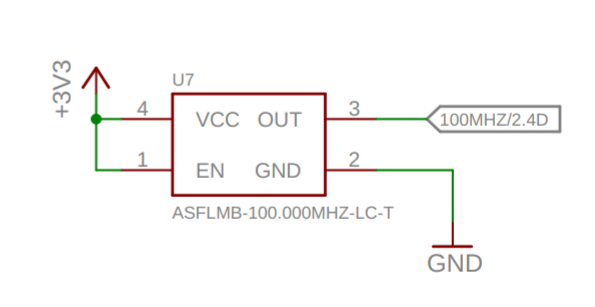
The answer to the first question is mostly straightforward. For the Alchitry Au, the 100Mhz master clock is generated using an Abracon ASFLMB-100.000MHZ-LR-T Low Voltage CMOS (LVCMOS) oscillator that is powered by a 3.3V power source.
From the Abracon ASFLMB Data Sheet 100Mhz is pre-programmed at the time of manufacture, the temperature grade (L) is -40degC to +85degC, the stability (R) is +/-25ppm, output load is blank - so 15pF, and came in a (T) 1000 piece reel.
With a clock stability of +/- 25ppm, the clock frequency will vary +/-250Hz over the operating temperature range - or about 0.000025% [25 / 1e6].

If we were using this clock in a real-time application, we could expect to gain or loose 24*60*60 = 86400s/day * 0.000025 = 2.16 seconds per day. Not quite as accurate as the typical 20ppm watch crystal, but still pretty good.
Output voltage will swing between not less than 0.8 Vdd (for HIGH) and not more than 0.2 Vdd (for LOW), so 2.64V (or above for HIGH) to 0.66V (or below for LOW). Rise and fall times at 15pF load are on the order of 1ns - about 10x faster than the nominal 100Mhz for this installation.
Connection to the FPGA:
On the Alchitry Au, the master clock is connected to pin N14 (IO_L12P_T1_MRCC_14) of the Xilinx XC7A35TFTG256 FPGA. Before more can be said about this input, we have to know more about how the FPGA clock distribution is accomplished within the chip.
The external connections to the XC7A35T FPGA are divided into 6 banks, labeled 14, 15, 16, 34, 35 & "GTP Quad 215". The numbered banks are of the "HR" type (see below). The GTP Quad bank is a collection of high speed serial transceivers, supporting line rates between 500 Mb/s and 6.6 Gb/s, that can be used to implement protocols such as PCI Express, SATA, SDI and others.
These FPGA architectural banks are not to be mixed up with the "A", "B", "C" and "D" bank connectors on the Au circuit board.
On the FTG256 package, Only banks 14 and 15 have their I/O pins fully exposed to the world. Bank 34 is only partly exposed. Bank 16 and "GTP Quad 16" are not exposed.
Some nomenclature to help demystify the abbreviations:
- HR: High Range - HR I/O banks can be operated from 1.2V to 3.3V
- HP: High Performance - HP I/O banks are optimized for operation between 1.2V and 1.8V.
https://www.xilinx.com/support/documentation/application_notes/xapp520_7Series_HPIO.pdf
- SRCC: Is a Single Region Clock Capable pin. As name indicates, these pins can route the clock input in the same clock region.
- MRCC: Is a Multi-region Clock Capable pin As name indicates, these pins can route the clock input to multiple clock regions - that is MRCCs can access multiple clock regions and the GLOBAL clock tree. MRCCs function the same as SRCCs and can additionally drive multi-clock region buffers (BUFMR) to access up to three clock regions.
- CMT: Clock Management Tile. Each CMT contains one MMCM and one PLL as well as input and output buffering for the clocks. The clock management tiles (CMT) provide clock frequency synthesis, deskew, and jitter filtering functionality.
- MMCM: Multi-Mode Clock Manager
- PLL: Phase Locked Loop
- BUFG: A buffer connected to the GLOBAL clocking tree.
- IBUF: An input buffer.
- HROW: A horizontal row connection within a region
The GLOBALLY connectable clock inputs on bank 14 are:
- IO_L12P_T1_MRCC_14 is the positive connection for the ***primary*** GLOBAL clock input into bank 14 (used for single ended clock input)
- IO_L12N_T1_MRCC_14 is is the negative connection for the **primary** GLOBAL clock input into bank 14 (used for differential clock input)
- IO_L13P_T2_MRCC_14 is the positive connection for the **secondary** GLOBAL clock input into bank 14 (used for single ended clock input)
- IO_L13N_T2_MRCC_14 is is the negative connection for the **secondary** GLOBAL clock input into bank 14 (used for differential clock input)
 |  |
Each numbered bank has a Clock Management Tile (CMT) with two clock connections that can be either single ended, or differential inputs. The MRCC connections can be connected to the GLOBAL clocking network of the FPGA.
The Au uses a single ended clock connection. Later when the Xilinx Vivado clock configuration wizard tool is discussed, we'll see that this second input can also be used in the design.
How is the FPGA configured to use this particular clock input?
Like most things FPGA, there is no "free lunch". Everything must be configured, connected or specified. Some of this complexity, such as connection routing described by the HDL, is taken care of by the synthesis tools (in this case Vivado). At a fundamental level, even the synthesis tools need to be told what's what - and that's where constraint files come into play. The constraint files
While a complete description of constraint files is beyond the scope of this article, the sections that pertain to clocks - particularly the master clock input - is relevant.
For our purposes of working in the Alchitry Labs environment, there are two kinds of constraint files:
1. ACF (Alchitry Constraint File) - which conveniently describe the mapping of Alchitry board signal names to particular pin inputs on the supported FPGA.
2. XDC (Xilinx Design Constraints) - Xilinx which
At a higher level, the Alchitry Labs IDE's simplified syntax does some of the work at build time by translating the ACF files to an XDC equivalent, which in turn is passed through to the synthesis tools.
The general format of the ACF file is pretty simple.
<ACF command> <signal name> <Board Signal | FPGA pin>
where:
- <ACF command> can either be "pin" to assign signal names to Board Signals, or "clock" to declare signal names as clocks.
- <signal name> is the name to be used as an argument in your top level module definition.
- <Board Signal> is the Alchitry Labs signal name listed in the circuit board's bank name ("A", "B", "C", "D") or one of the special names for CLOCK, RESET, ADC, SPI, USB, I2C or DDR interfaces.
While not outwardly documented, the Board Signal names and their translated FPGA pin names can be found here:
In the alchitry.acf file we can see that signal clk0 is defined and assigned to CLOCK. CLOCK in turn is translated to FPGA signal N14. We also see that the signal clk0 is set to be a clock input of 100Mhz.
pin clk0 CLOCK;
clock clk0 100MHz;
Here is where we have to be honest with ourselves. The clock can be defined to be any value, not just 100Mhz. Since the master clock input really is 100Mhz, declaring it to be some other value in the ACF file would cause undefined behavior. This is because the synthesis tools rely on this value being accurate to generate internal timings. Also if there are other design or FPGA modules that depend on an input of a particular frequency, they will not operate as expected. Thankfully, the synthesis tools will compile the lower level modules first and in the case of using the Clock Wizard tool to control a clock management tile generating alternate clocks, will flag an input frequency discrepancy.
At build time, the alchitry.acf file is translated to alchitry.xdc, a Xilinx XDC file. The section pertaining to the clock is:
 # clk0 => 100000000Hz
    create_clock -period 10.0 -name clk0_0 -waveform {0.000 5.000} [get_ports clk0]
    set_property PACKAGE_PIN N14 [get_ports {clk0}]
    set_property IOSTANDARD LVCMOS33 [get_ports {clk0}]
Here's what's happening:
# clk0 => 100000000Hz
Is just a comment to say that signal clk0 is 100Mhz.
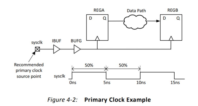
create_clock -period 10.0 -name clk0_0 -waveform {0.000 5.000} [get_ports clk0]
Declares a primary clock named clk0_0 with a period of 10ns (100Mhz) with a 50% duty cycle, no phase shift, and will be connected to the signal named clk0. create_clock must be declared first, so other properties can be assigned to it. A primary clock can only be defined by the create_clock command.
set_property PACKAGE_PIN N14 [get_ports {clk0}]
Associates the signal clk0 with pin N14 (our clock input) of the FPGA. Since N14 is a MRRC (Multi-region Clock Capable) input, it can be used as a primary clock input.
set_property IOSTANDARD LVCMOS33 [get_ports {clk0}]
Sets IOSTANDARD to use on the the top-level input port associated with signal clk0 - in this case 3.3 Volts (LVCMOS33) nominal for pin N14. You must specify an IOSTANDARD on all ports used in a design, which is why you'll see this for other declarations in the achitry.xdc file generated by Alchitry Labs from the alchitry.acf file.
Because this is a primary clock, it will be connected by the synthesis tools to the GLOBAL clock tree through an input buffer and a GLOBAL clock tree buffer.
In summary, N14 is defined to be the clock input and the constraint files tell the synthesis tools how it's connected.
How is this clock made available to other FPGA resources?
Like all Series-7 Xilinx FPGAs, the XC7A35T used on the Au board is divided into regions. The the clocking backbone divides the device into left and right sides while the horizontal center line divides the device into top and bottom halves.
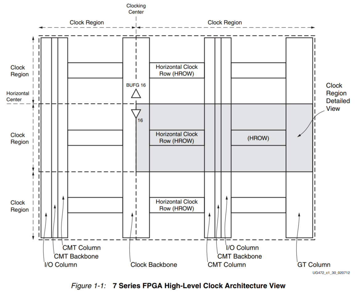
The resources in the clock backbone are mirrored to both sides of the horizontally adjacent regions, thus extending certain clock resources into the horizontal adjacent region.
All horizontal clock resources are contained in the center of the clock region horizontal clock row (HROW), and vertical, non-regional clock resources are contained in either the clock backbone or CMT backbone.
The top and bottom division separates two sets of global clock buffers (BUFGs) and imposes some limitations on how they can be connected. However, BUFGs do not belong to a clock region and can reach any clocking point on the device.
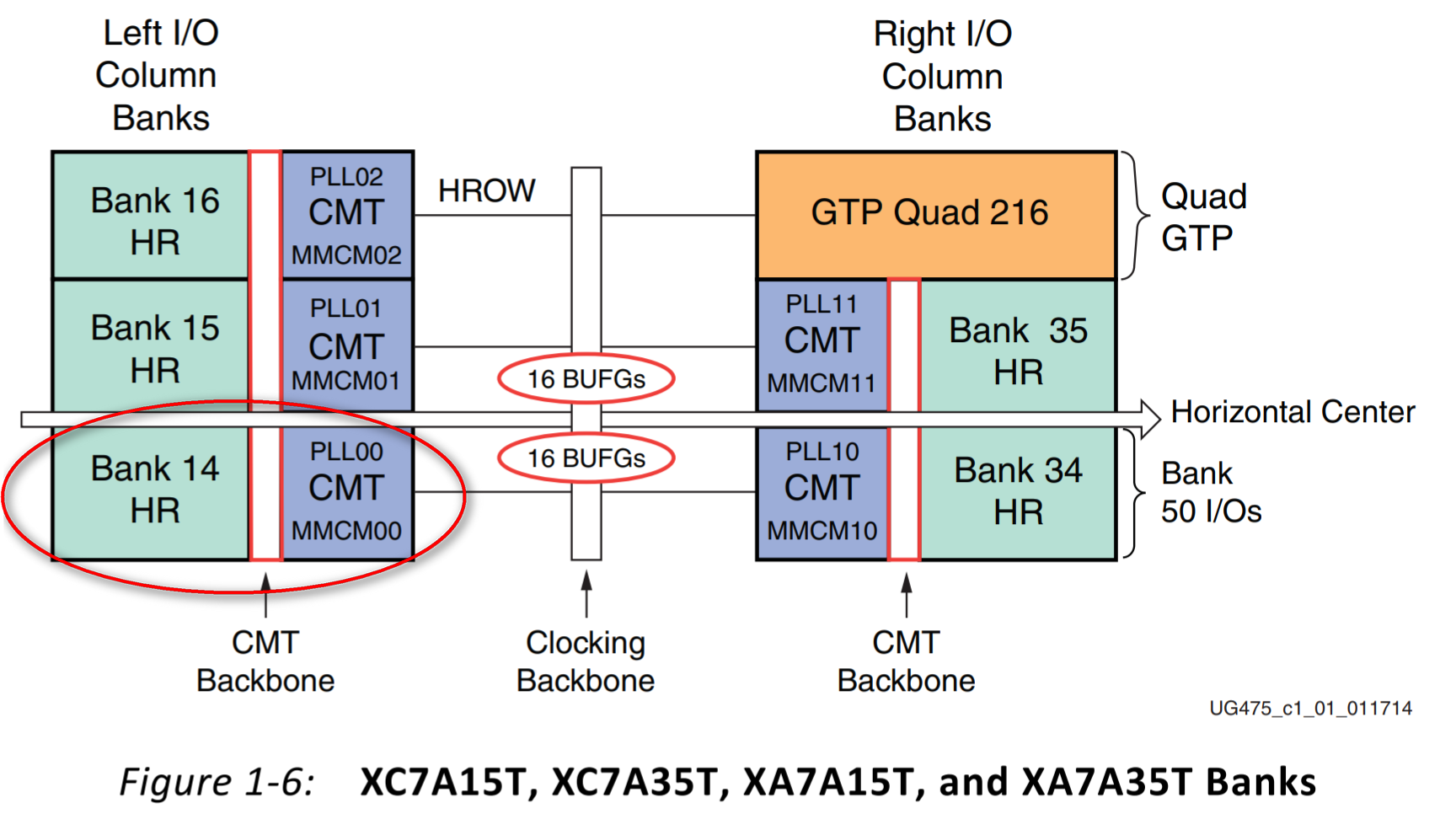
Our 100Mhz master clock is connected to pin N14, which is in Bank 14 and can be connected to CMT0 (and it's MMCM or PLL modules) via the CMT backbone.
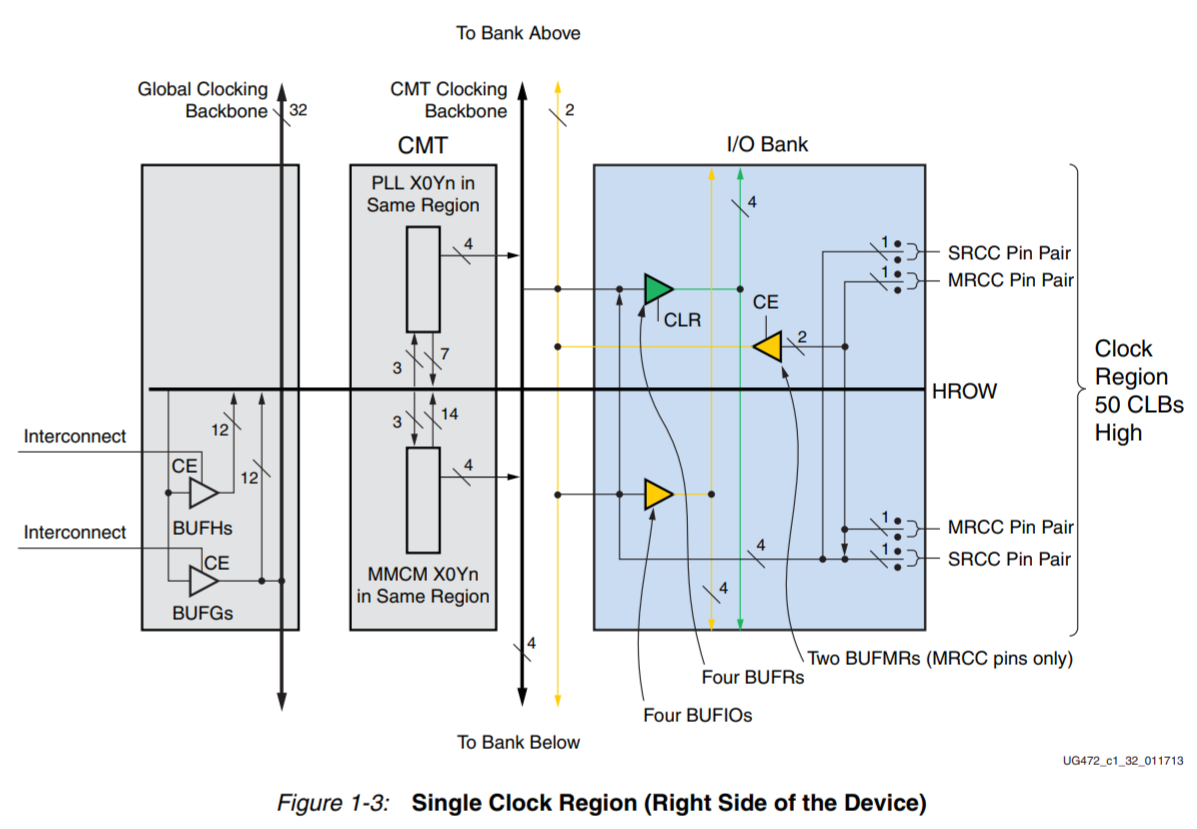
From there, the MMCM (or PLL) output can be connected back to the clocking backbone by a GLOBAL buffer (BUFG) along an HROW and distributed to the rest of FPGA.
The clock input pin is routed through an input buffer (IBUF) and a BUFG.
How can other clocks be synthesized from the master clock and distributed within a design?
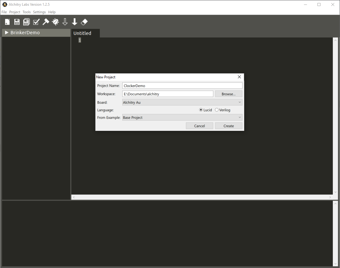
So here is where the rubber meets the road from a practical standpoint. We'll start off by creating a new base project in Alchitry Labs - I'm calling it ClockerDemo.
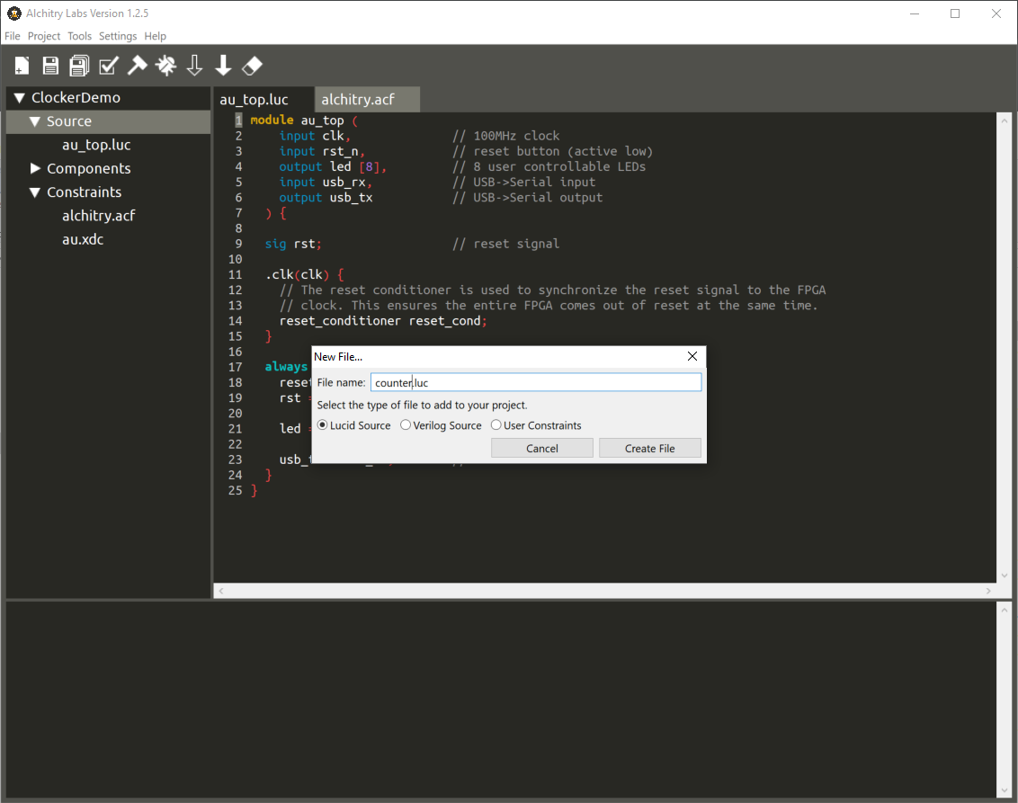
Next we'll create a new counter module to be driven by the clock of our choosing. This one I'm just calling "counter".
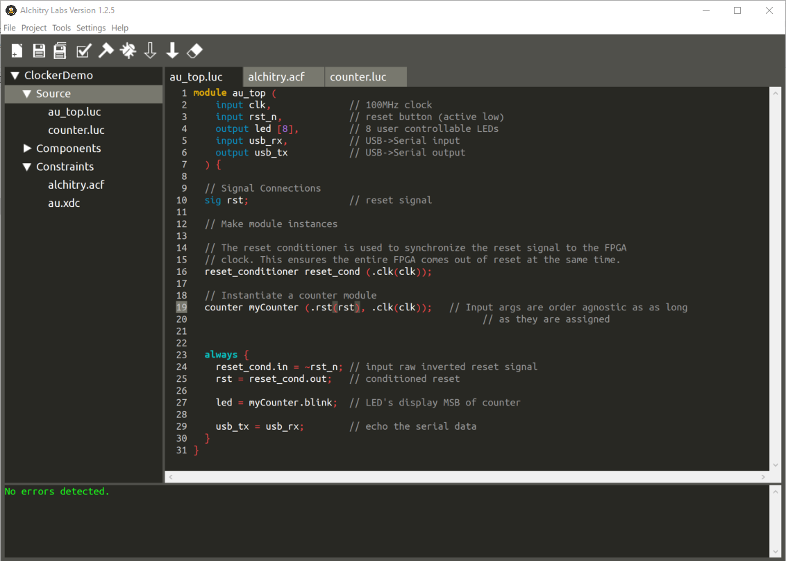
The code for the counter module looks like this, and is a 32 bit counter, driven by the clock of our choosing with the 8 most significant bits being returned for later display on the Au LEDs.

The top module declares an instance of the counter and connects to the LEDs.
Build the project and upload to the Au. You should see the counter display on the LED's at a fairly good rate, since it's being currently driven directly by the 100MHz primary clock input.
MAKING THE NEW CLOCK
We're going to create a new clock component that uses one of the CMTs (Clock Management Tiles) to generate a new clock from the primary clock input. To do this we're going to launch Vivado from AL's Project --> Vivado IP Catalog menu.
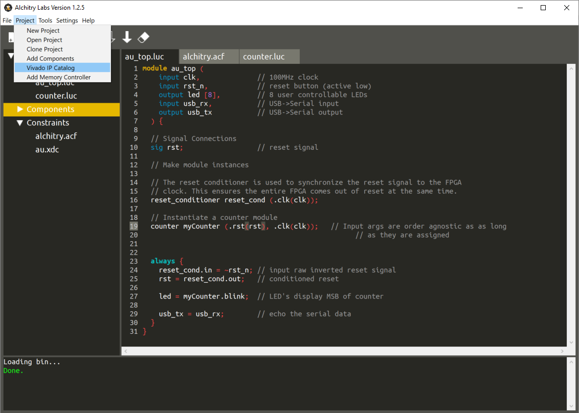
Vivado should launch and show it's IP catalog. Scroll down to FPGA Features and Design, choose Clocking, then double click Clocking Wizard to launch.

The first thing to do is to name you're component. Although you can come back to edit later, the initial name is a one-shot deal. You won't be able to rename the component after it's been initially generated.
For this demo, I just chose to get rid of the "_0" suffix and call it "clk_wiz".
On the Clocking Options tab, just leave the selections alone. You can choose between using the MMCM or the PLL module - both have some minimum frequency differences - and I'll leave that for your to explore on your own. We are doing Frequency Synthesis, so leave that checked. Phase alignment with the input clock is not important for this demo, so leave that checked as well.
The Input Clock Information is also set up for us, however I'm going to edit the port name for the Primary Input Clock to just "clk_in". The MMCM module will be expecting a 100MHz input signal, and is coming from the Single-ended clock capable pin, N14
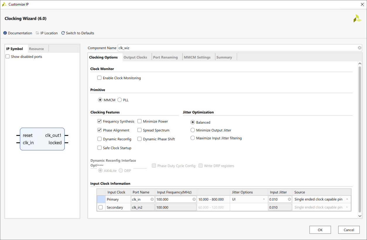
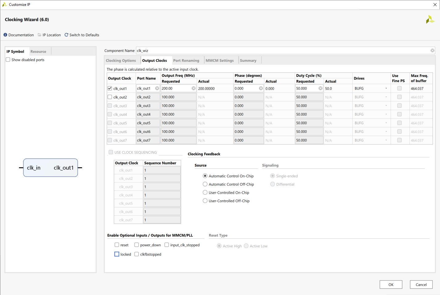
We'll be driving the GLOBAL clock bus, so leave the drive set to BUFG.
At the bottom of the screen we can delete the optional RESET input and LOCKED output.
There are no ports or pins to rename, so nothing to do on the Port Renaming Tab. Likewise we're not going to override any of the Wizard settings in this example, so leave MMCM Settings alone as well. If we used the PLL, this tab would give us the opportunity to override the PLL configuration as well.
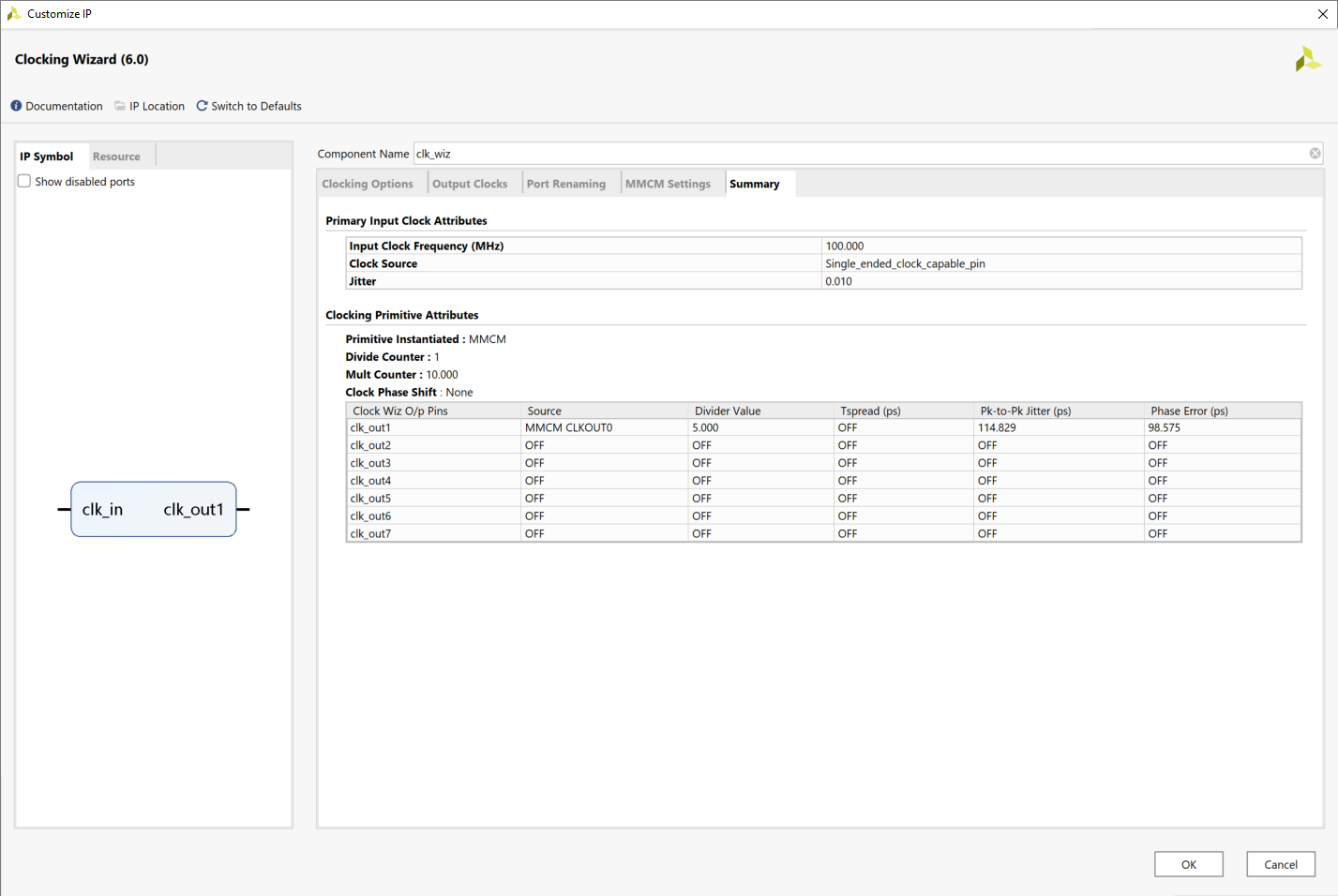
Finally, the Summary Tab will show the final results of our configuration.
- Based on the options chosen, the Clocking Wizard automatically chooses the correct clocking primitive for a selected device and configures it based on user-selected clocking features.
Hit OK , then Generate in the pop-up to build the files for our shiny new clock module. I will take a little while, so wait for the process to finish - then just close Vivado.
After returning to AL, you'll see that a new core has been generated that defines our new module "clk_wiz".
Now - lets connect that new clock module into our project.
Since the new clock module's input is driven by "clk", which is the primary clock input connected to N14 of clocking region 14, it can be presumed that the MMCM00 module of CMT0 will be chosen by the synthesis tools to drive the module.
Build and upload these design revisions and you'll see that our counter is going at twice the rate it was.
You can right-click on the clk_wis_stub.v file in the cores list to re-launch Vivado and edit the clock configuration in case you need to make changes. Just be sure to re-generate the clock module IP in Vivado and rebuild the design in Alchitry Labs.
Closing
I hope you enjoyed reading this article and that it helps demystify setting up alternate clocks for your Alchitry Au project.
Cheers,
MDL
Credit where credit is due.
Below - sources of information for this article
7 Series FPGAs Packaging and Pinout
Frequency Stability - Everything RF
7 Series FPGAs GTP Transceivers
Abracon MEMS Clock Oscillator Data Sheet
Alchitry Labs - Source Code on GitHub
Xilinx Artix-7 FPGA Data Sheet
Discussions
Become a Hackaday.io Member
Create an account to leave a comment. Already have an account? Log In.