 Wancheng Zhou
System Hardware Platform
The hardware of this firmware upgrader should own many common communication interface, meanwhile, it must own fast storage interface such as SDIO, USB HOST. In this case, the storage media will be SDHC / TF card since it is very common, and can be embedded on-board. A good product should put user experience as the most important factor, even though it may be tough for hardware and firmware design.
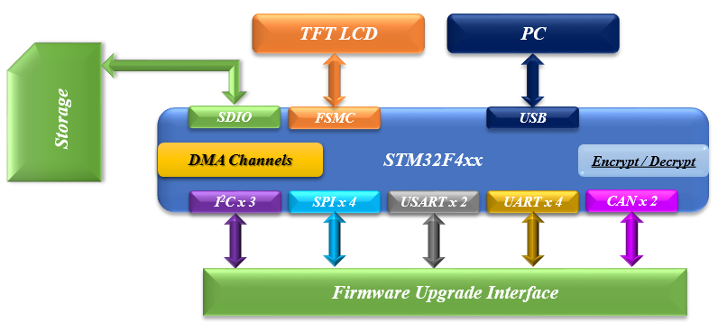
Based on considerations above, the core MCU / Micro-controller is chosen from ST-Cortex M4 Series, take STM32F407IGH for example, it has abundant peripheral devices, except for the common communication interface above, it owns USB-OTG (Host / Slave), FSMC (Flexible Static Memory Interface), DMA (Direct Memory Access – makes data transmission more efficient), not to mention that it also owns hardware encrypt / decrypt units which are definitely essential for firmware release. See Figure 2.1 for more information.
Note that, Ethernet is not a common firmware upgrade interface, furthermore, the Ethernet physical chip is large and expensive. From the "Cost-Effective" purpose, it is excluded from the block diagram, but it can be added at any time since STM32F4 itself owns hardware Ethernet even though it needs external PHY.
STM32F4xx Virtual USB Disk Development
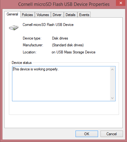
With STM32 official USB library (v2.1.0) (MSC Device Class) and SDIO Hardware Interface, virtual U disk can be easily implemented. The purpose of this design is to simplify user operations, even though user can pull the SD card out of upgrader and store firmware data directly into it. Furthermore, from the purpose of product development, it is better to hide design details. What's more, in the future, we can use eMMC chip (8-bit SDIO mode) or FLASH (with FSMC) with smaller size to make it more compact.
Meanwhile, with this design, a corresponding client software can be developed to fetch the latest firmware from GIT management system. To do this, we need to change the USB-MSC name so that it can be easily identified by the client software. Specifically, the USB storage inquiry data region should be modified.
SD Card Speed Test and R/W Operation with FatFs
Currently, I used USB-FS mode which can achieve 12Mbps ( 1.5MB/s ) R/W performance. It is acceptable to store small-size firmware data. USB-HS mode can be implemented with USB3300 phy to achieve much higher performance.
Note that there exists 2 factors that may impact the firmware upgrading speed:
- How fast it can retrieve data from PC ( when connected to PC, USB FS speed and SD card RW speed can be the limitation );
- How fast it can upgrade the target device through any communication interface ( interface dependable, such as UART, I2C, CAN etc. ).
After test, it turns out that compared to USB-FS speed, SD card R/W speed is much faster ( SDIO - 4bit mode ) with FatFs. And the upgrading speed is completely dependent on interface speed.
The speed test of SD card is shown below:
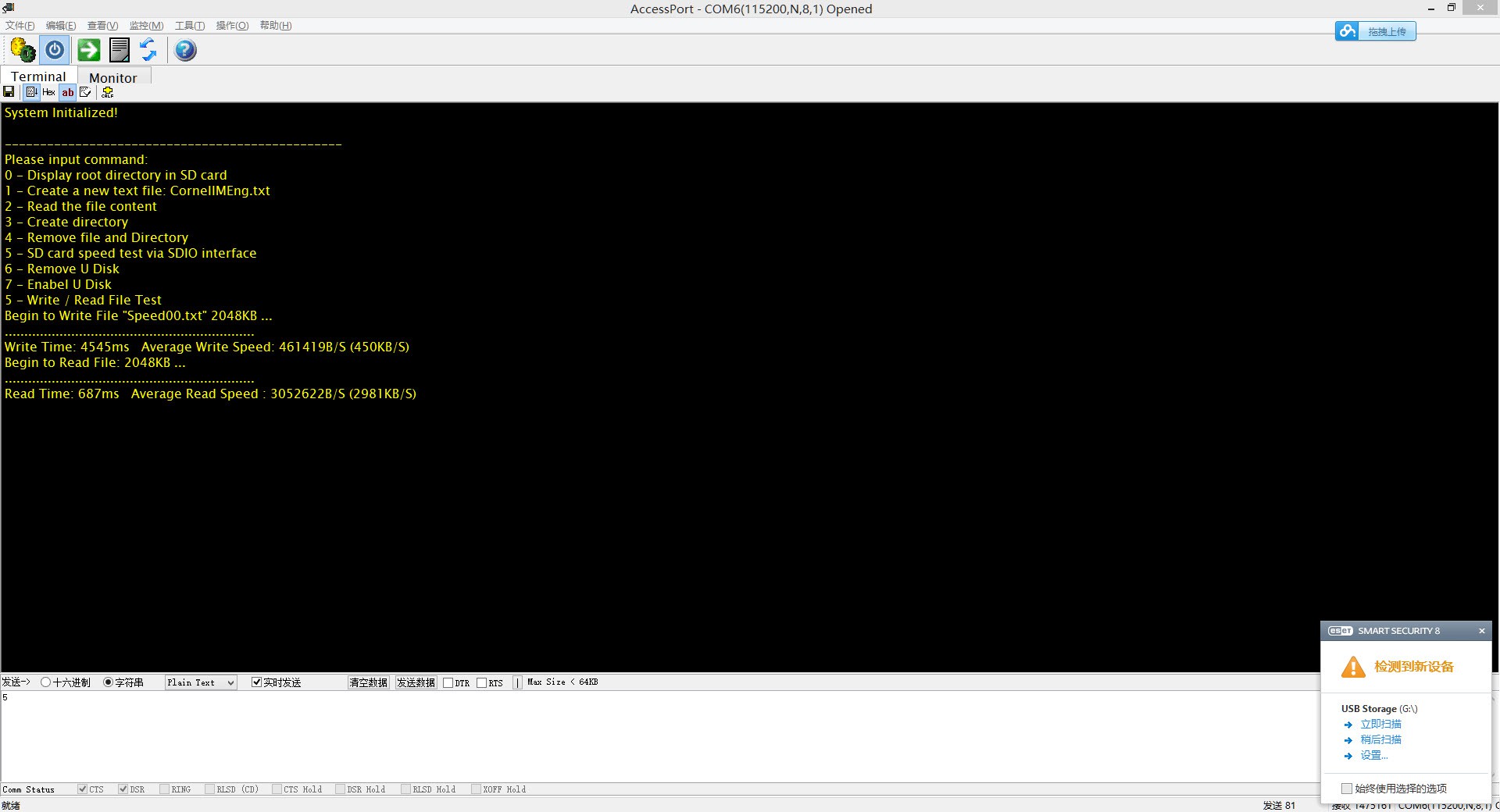
If the SD card is empty, the write speed can be very high, not to mention the read speed. I added data validation process, so it is a bit slower, but it can be still up to 3MB/s.
SMART LINK Protocol Development
The communication protocol should be able to perform basic master and slave messages (functionalities) described below:
- lRequest / Response firmware upgrade
This message is used to check device connection or device status, when slave receive this message, it should response to master based on specific command.
- lRequest / Response firmware transmission
This message tells slave device that the firmware data is about to transmit, when slave receives this message, it should respond with the maximum firmware segment size (internal RAM size) it supports.
- lRequest / Response firmware raw data transmission
Master send this message to inform slave device to prepare to receive firmware data. After slave successfully receives the data and program the firmware data into flash, it should response to the master to report the programming results.
Note that the difference between Master and Slave is not absolute. If module B is connected to the upgrader indirectly via Module A, then Module A should be able to perform all master functionalities to Module B in order to perform indirect firmware upgrade.
Now that all the basic functionalities are defined, the protocol package format must be carefully designed to meet encryption and package checksum requirements. Also, it must be able to be applied in either Peer-to-Peer or Bus connection. The package anatomy is shown below:


Protocol Version A is suitable for those interfaces which support "Multi-Host" and the low-layer protocol itself can distinguish different communication peers. For instance, CAN low-layer protocol contains "Arbitration Field" which is composed of "Identifier" and "RTR (Remote Transmission Request) bit". With this field, we can easily identifier the message sender even though this field is actually used for communication arbitration (CAN Specification 2.0B).
Compared to protocol version A, version B is kind of verbose. However, this kind of protocol format is necessary for those "Peer-to-Peer" communication interfaces. Furthermore, this protocol can be used for "Sub-Module" Firmware Upgrade. For instance, if a module (module X) is impossible to be connected to the external interface, but it communicates with one of the modules (module Y) that connects to the upgrader. In this way, upgrader can send X firmware to Y, and Y upgrades X indirectly.
Both Protocol A and Protocol B are implemented with CRC-8 / 16 checksum filed to enhance the communication safety. What's more, it is also designed for software convenience: if the "Header CRC8" is wrong, the whole package can be ignored.
After the package format and functionalities are defined. It must be verified to make sure that all request / response message can be correctly generated. To achieve this, a software Test-Bench based on Visual Studio VC++ is created to explicitly verify Smart Link.
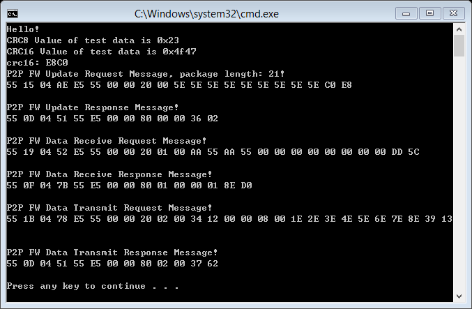
Figure above shows the results of P2P message (Protocol Version B) validation, As soon as it passed the validation, the next step is to utilize the Smart-Link: It must be lightweight, be compatible to most popular C compilers and be efficient. To achieve this, a "Header File Only" Smart Link is further designed to meet these requirements. Specifically, inline functions are widely used in Smart Link. The purpose of inline functions is to achieve the same performance as macro function, and it can also be further utilized based on different C compilers. For instance, to avoid the compiler not to inline the functions, some C compilers let users to use some special assignments to force the function to be inlined (__attribute__( ( always_inline ) )). The core function that will affect the protocol efficiency would be the function which is used to decode the message. Considering the compatibility and mobility, the function should be called continuously as long as the interface receive buffer is not empty. The state-machine of decode function is shown below:

AVR Bootloader Design Based on SMARTLINK
To verify the upgrader, a test bootloader must be designed. In this project, the AVR board (ATmega16) used in ECE4760 to verify the basic functionalities of firmware upgrader. This AVR bootloader is also a demonstration on how to use Smart Link protocol. To start with, the AVR bootloader region and size must be clarified. The flash region allocation for ATmega1284p is shown below:
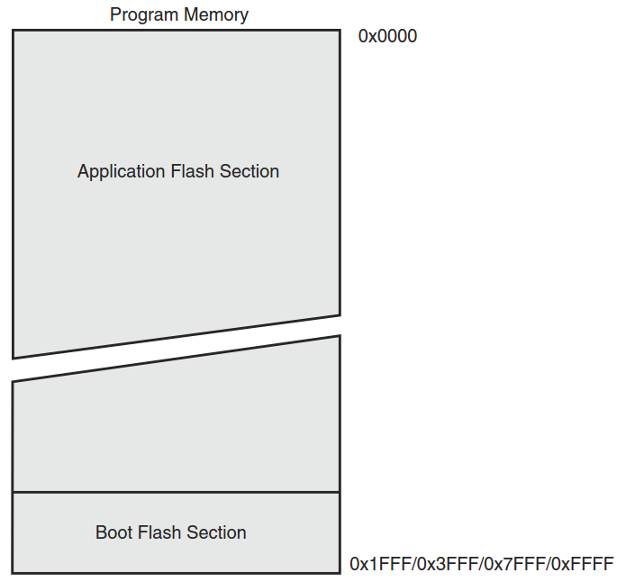
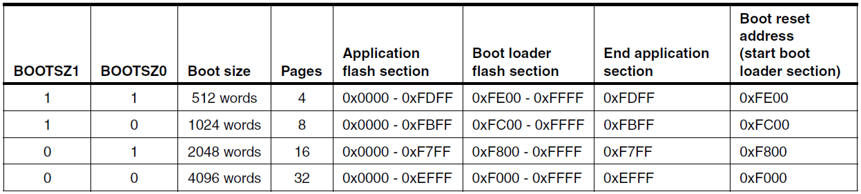
From the figure above, we can see that the boot flash section is at the bottom of the flash. All we need to do is to make sure the bootloader code is within appropriate size. Once we define the bootloader start address, memory location should be assigned for ISP programming. According to ATmega1284p datasheet, the maximum bootloader size is 4096 bytes (4KB), this means that the size of bootloader application cannot exceed 4KB. It is a good way to validate the Smart Link protocol to see whether it is "light" enough or not. Figure below shows the FUSE configuration for bootloader size selection.

GUI Design ( Not Necessary for Future Productization
To make it much easier to use, a simple GUI is created to allow users to operate the firmware upgrader easily. The basic functionalities designed in this demo includes "Browse SD", "Connect PC", "SD Speed Test", "Connect Device" and "Upgrade Device". The whole GUI's color scheme is designed based on WinXP style. Shows the simple GUI interface.

The TFT-LCD main controller used in this project is RA8875 which owns 768KB DDRAM. Generally, operating the LCD equals to operating the display RAM. STM32F407 owns hardware FSMC (Flexible Static Memory Interface) which can be used to efficiently write to or read from the DRAM. All we need to do is to assign the address for the display RAM. The address for display RAM is actually defined by hardware connection and the BANK region of FSMC mapped memory. In this project, the RS signal (write register or write RAM data) of RA8875 is connected to FSMC_A18, note that in 16-bit mode, the internally generated hardware address HADDR [25:1] is actually the value of hardware FSMC address line A [24:0] (See Figure below).
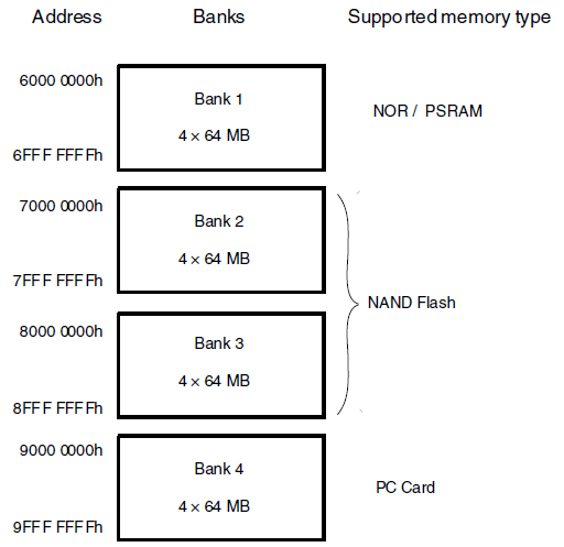
In this scenario, FSMC_A18 is corresponding to the address HADDR [19]. Also, we selected address 0x6C00_0000 of FSMC Bank 1 (starts from 0x6000_0000) for display address (STM32F4xx User Manual Table 168 Note). Then the actual address for RA8875 registers is
0x6C00_0000 + (1 << (18 + 1))Then I can simply define a private macro definition to either send CMD or DATA to LCD module.
#define RA8875_BASE            ((uint32_t)(0x6C000000 | 0x00000000))

/* FSMC 16bit Mode, A18 is mapped to HA19, and A18 is connected to RA8875 RS pin */
#define RA8875_REG            *(__IO uint16_t *)(RA8875_BASE +  (1 << (18 + 1)))
/* FSMC 16bit Mode, normal address */
#define RA8875_RAM            *(__IO uint16_t *)(RA8875_BASE)

#define RA8875_RAM_ADDR        RA8875_BAS
Summary
In this project, an efficient firmware upgrader was designed and could perform firmware upgrade to target device based on IAP methodology. Multiple interface drivers are designed to verify system efficiency. From this project, we can see that a good embedded system is not only needs qualified hardware, but also requires good firmware design. Good firmware design sometimes can make up hardware defects, and slight hardware modifications can make the software design easier. For embedded system design, both hardware and software are scalable.
Github Link for SMARTLINK will be posted later.