 István Hegedűs
The idea of the project came when my 30 years old Commodore Plus 4 has suddenly died and I suspected that TED was the main cause. After an extensive troubleshooting it turned to be that the 8551 ACIA chip was the guilty one and I have fixed it, however by that time this project has been born in my head. I have checked the internet and was surprised that no one has created a TED FPGA core before.
Although there are some TED documents available on the internet, they are incomplete, not precise and do not fully describe the inner secrets of the chip. There is no point in creating a chip which is not cycle exact, doesn't emulate TED scan lines and events properly. An extensive research started on the hardware using own written test codes, logic analyzer, oscilloscope and source code analysis of Plus 4 emulators. I quickly realized that due to the inner multiplexed architecture of TED certain events are initiated at the specified time (described in 7360R0 preliminary data sheet) however they happen later in time after 1-2 single clock cycles. This behavior was emulated in certain emulators like Plus4emu, which made the emulator code much more difficult to understand.
Two years of analyzing the hardware, documents and code writing has led me to a working TED chip which is capable of running most of the programs and demos the same way as the original hardware. The project is not finished though, I am planning to refine it further and make it available to everyone.
The code is written in verilog language and uses Gadget Factory's Papilio One 500k developer board. This board has a Xilinx Spartan 3E 500k FPGA which is more than enough for implementing a whole Commodore computer except its main memory. The FPGA has only about 40Kbyte RAM which is not enough for a 64Kbyte computer especially if we think of the 16K Kernal and Basic ROMs. The TED core module doesn't use any Xilinx specific HW blocks or macros so it is very easy to reuse on other Vendor's FPGAs. Later on I have continued the development on the more advanced Papilio Pro board with Spartan6A FPGA and onboard sdram. Although I wanted to implement the TED chip , it was clear that I need to implement other supporting components (CPU, ROM, keyboard matrix) to test the chip on the FPGA board. As several 6502 CPU FPGA codes exists I did not want to reinvent the wheel and decided to use a publicly available one which has illegal opcode implementation also. I have chosen Peter Wendrich's 6502 vhdl code from the fpga64 project. Peter has confirmed via email that I can use the CPU part of his code for my FPGATED project and include its source in FPGATED sources.
Papilio TEDwing
First step of the project was to create the hardware developer environment, which means building a suitable wing board for the Papilio One FPGA board. Gadget Factory has already created an Arcade Megawing however it lacks the memory part which is crucial from the TED system's point of view. It was however a good starting point for the TEDwing design. These were the main design criteria for the Papilio TEDwing:
- 12 bit VGA/RGBS output
- 2x 4464 DRAMs
- IEC serial bus connector
- PS2 keyboard connector
- Stereo audio out with low pass filter
- RS232 serial output
- Reset button
- Jumper to configure VGA or RGBS mode
The board schematic was inspired by the following other designs
- VGA, audio and PS2 part from Papilio Arcade Megawing
- IEC serial bus from SD2IEC design
- DRAM from Quickswitch QS3 voltage level translation application note AN-11A
- RS232 from MAX232 application notes
I have used Eagle 6.2 to create board schematic and layout. Size of the board fits to the limitation of Eagle free edition. All traces of the PCB was manually routed by me then sent for manufacturing. SMD soldering of components were done by me without hot air gun.
The above mentioned features fully utilize free Papilio I/O ports so there is no space left for joystick connections or user port. This is a small drawback however the original goal was to create only the TED chip which doesn't require these.
VGA/RGBS port uses resistor ladder for the D/A converison and provides 4096 color voltage levels which is more than enough for the 121 colors TED can produce. The display output can be used in two modes, selectable by a jumper onboard; VGA or RGBS (this feature is not implemented at the moment). VGA has the same pinout as a standard VGA connector so a normal VGA cable can be used to hookup to the monitor. It requires however a scandoubler inside the FPGA which is not yet implemented (as of today VGA mode is not usable). RGBS mode provides NTSC or PAL compatible RGB video signal that can bee hooked up to a vintage monitor like the one I am using Philips CM 8833-II or a Commodore 1084(s). This requires a special VGA to Scart display cable which has the same wiring as the one used for Minimig. FPGATED provides clear, sharp picture on scart monitors and normal TV sets. It reproduces TED's horizontal and vertical sync signals precisely.
As internal memory of the Papilio One platform is not enough to implement a 64Kbyte computer with is 32Kbyte ROMs, external memory was needed. When I started the project I did not have a Papilio Pro board which has external memory installed so I decided to add DRAM to the wing. As the plan was to create cycle exact TED implementation, the best choice is apparently the same or similar DRAM chip used back in the days. Placing 8x 4164 DRAM chips on the tiny area of TED wing was not possible so I decided to place 2x 4464 chips which provides the same functionality and its memory control is the same. This chip however is a 5v IC so a voltage level translation was needed. As the memory's RAS, CAS and address signals are only inputs from the dram point of view, the FPGA's 3.3v LVTTL compatible output can drive those pins without translation (it works fine). Only the bidirectional 8 data pins needed voltage level translation for which I have used one Quickswitch IDTQS3245 bus switch IC. The Quickswitch application note describes well how to use it for voltage level translation, it needs about 4.3v Vcc for proper 5v to 3.3v level translation. This can be achieved by using an 1N4148 diode between Papilio board's 5v pin and the IC's Vcc pin. See below figure for the voltage translation part.
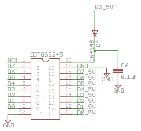
Figure 1. Voltage translation for external DRAM
Note that on my TEDwing 1.0 version I have forgotten this diode so on the PCB photos a quick fix modification can be seen for it. In latest 1.1 schematic and PCB layout I have corrected this mistake and added a SOD323 diode on the backside of the PCB.
Memory address multiplexing is done inside the FPGA.
IEC serial bus was needed in order to be able to load software from floppy and test FPGATED. As the Commodore 264 series computers handle the IEC bus from software, its implementation is fairly easy, I just had to make sure that an open collector output drives the 5v bus and the incoming signal is voltage level translated to 3.3v. These signals can be connected to the internal CPU's I/O ports. In real hardware this is done by a 74ls06 IC which would work here also however the incoming signal's voltage level shifting would be still needed. I decided to use the same solution as in SD2IEC project available on the internet. In order to spare board space, instead of 4 FET transistors I decided to use 2x IRF7103 ICs which contain 2 FET transistors each thus simplifies the design. The solution works perfectly and communicates with real 1541 drives and SD2IEC drives very well.
TED module
Main goal of this project was to create the TED module (ted.v). From the beginning my intention was to make it one day a drop in replacement in the 264 series computers, thus the module's input/output ports reflect the main signals of the original IC. Figure 2 shows ted module's ports.
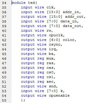
Figure 2. TED verilog module's input/output ports
As it can be seen this is still an internal module from FPGA's point of view thus bidirectional signals like address and data buses have an in and out ports. These signals can drive a tri-state buffer on an IO block when they leave the FPGA. Obviously this module cannot be used as a drop in replacement because some signals are not exactly the same as the original IC has.
First of all the main clk signal is not the same 14MHz NTSC ( 17MHz PAL) one that the original IC needs, but rather an FPGA DCM produced 4x dot clock signal (28.63636 MHz for NTSC and 28.288 MHz for PAL). The reason why I have chosen to use these frequencies is simple; all required TED internal frequencies can be produced easily from them via counters, while they give high enough resolution for handling internal events (like hold time emulation, delays, memory controller events). This has only one main drawback, TED module's internal pal/ntsc register bit doesn't change the internal clock division as in the original IC (original TED divides main clock by 16 for NTSC and 20 for PAL systems to get CPU single clock frequency). In real life however a normal user never changes this bit in a configured PAL or NTSC system thus this difference is irrelevant. In future my plan is to solve this also. As the FPGA has more DCMs it is possible to create PAL and NTSC frequencies with different DCMs and choose between them based on the pal/ntsc bit.
Secondly the color output is a 7 bits digital value representing the pixel color using TED's palette values. This signal needs to be fed to an another module (colors_to_rgb.v) which will convert it to a 12 bit RGB value using a simple LUT. This differs from TED's Luma and Chroma analog signal so one mor ething to work on in the future.
The last non-usual signal is the cpuenable output which is used by an FPGA 8501 CPU as clock signal instead of cpuclk output. It generates an enable pulse for the FPGA CPU with single or double cpu clock frequency and is in synchron with cpuclk output. This is needed because the FPGA CPU uses the same main clock as TED module while the CPU needs much slower speed. One can decide to use an external original 8501 CPU with FPGATED thus cpuclk output is generated as well. Xilinx synthesis software will remove the not needed (not connected) cpuclk or cpuenable signals during optimization.
TED's internal operation
Internal operation of TED can be discovered in several ways; reading available manuals and plus4 related mailing lists, software based tests with visual inspection, measurements using logic analyzer and oscilloscope, analyzing emulator source codes.
For hardware measurements I have used a 32 channel Open Bench Logic sniffer from Gadget factory and a Gwinstek 4 channel digital oscilloscope on a C16 mainboard. Reason for C16 instead of plus4 is that TED chip is much easily reachable on a C16 mainboard than on a Plus4. It makes a lots of difference when hooking up logic analyzer to the chip.
The following technical documents and resources were used
- mail archives/forums from plus4world website
- TED 7360R0 Preliminary Data Sheet
- TED Extra Pages
- TED System Hardware Manual
- TED Patent US4569019
- Service Manual Model Plus 4 Computer
Despite these resources several experiments were needed to understand how the chip works internally (and it still has some mysteries undiscovered).
Clocks
As already mentioned the FPGA is running on a 4*dot clock speed (clk) and a cycle counter (phicounter) counts 16 FPGA clock cycles which equals to the period of the double cpu clock (dphi). This is further divided to create a single cpu clock (phi). TED will switch the CPU's clock signal between phi and dphi at the proper time when needed. See figure 3.
Horizontal dot counter
Internally TED's operation is tightly pending on two main counters, horizontal dot counter and vertical line counter. Horizontal dot counter is the most important and the most confusing one. It is a 9 bit register and runs from 0 to 455 then changes to 0. When modified by user a negative true value needs to be written to it and higher than 455 number is accepted (because it is a 9 bits register). It will then run until 511 then overflows to 0. The user modification however does not have an effect on counter's bit 0-2. These first 3 bits of the counter are increased and the rest of the bits are latched from the data bus. It ensures that by modifying the horizontal counter phi0 is not phase shifted unintentionally. Some plus4 programmers mention however that the horizontal counter modification doesn't affect bits 0-1 only which my experiments did not prove.
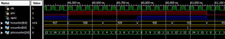
Figure 3. Generated clocks, Horizontal dot and Vertical line counters
Several internal events/timings are based on the horizontal dot counter value described in Preliminary Data Sheet, however confusion comes when we do measurements and experiments on the real hardware. Some events seems to happen at the right time, others seem to be delayed by one single clock period (single clock = 894.89 KHz for NTSC and 887 KHz for PAL system). Horizontal dot number 0 is not the beginning of a scan line, it is the beginning of the window area (after left side border) and what makes investigation even more complicated is that emulators are not using the same dot numbers for these counters, rather a shifted version (Yape and plus4emu uses different representations). The two main plus4 emulators have certain events at different time positions not consistent with the documentation and each other. What a chaos! I decided to make my own reference so a lots of experiments and measurements lead to my version of horizontal events. In order to find a reference point in the event list and identify its horizontal position I decided to analyze the horizontal sync and the equalization pulses. Also a good reference point is the raster interrupt position which in theory happens at the beginning of each scan line. It seems these events happen exactly at the time described by the documents, however oscilloscope measurements has shown that slew rate of the signals takes 2 pixel clock periods so this must be takin into account. As FPGA slew rate is much faster this kind of shifting needed to be taken into account otherwise it has caused an unintended window position shifting on the screen. Thus several horizontal event positions in the source code are shifted by 1 pixel because that is half way between the high and low states of the original signal.
One key point is when the CPU writes horizontal counter what happens exactly. When will TED take the data from data bus and update the horizontal counter? My experiments with this counter has shown that it does not happen on cycle border (phi0 high->low transition) but rather with one pixel clock delay. This theory is consistent with the white pixel bug effect (when writing a color register will cause one white pixel at cycle border) and this same delayed writing can be used to emulate this bug. Implementing horizontal counter behavior perfectly is very important because most demos are manipulating it.
In FPGATED the hotizontal event positions are turning on a one FPGA clock cycle active flag which is used in several parts of the module to start/end certain events.
Vertical line counter
The vertical line counter behavior is much easier to understand comparing to the horizontal one. It has a key role in the PAL/NTSC standard picture generation. While in case of the horizontal counter the same event positions are used for both standards, the vertical line number events are different for PAL and for NTSC. It is not a big deal to implement these, TED register's pal bit chooses the correct line values for Vertical sync, Equalization pulses, screen blanking. However one key point for proper hardware emulation is that TED internally latches this counter at the beginning of each new line and uses that latched version for certain internal operations (like for generating raster interrupt). Thus manipulating the vertical counter has in several cases effect in the following raster line only. This is important because of some cool raster effects in demos and games.