 chris.coulston
One-Off Solder Mask
This document outlines how to take an EAGLE layout, a printed circuit board manufactured using the Protomat C60 circuit board cutter, Kapton tape (1 mil thick), and a Universal Laser VLS 3.50 to create a solder mask for your circuit board. Figure 1 shows the finished product; a cut circuit board covered by amber-colored Kapton tape forming a solder mask.
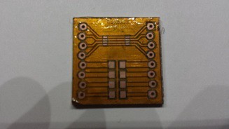
Figure 1: A circuit board fabricated using the ProtoMat C60 PCB cutter with a Kapton tape solder mask attached, leaving only the pads, vias, and lands exposed.
The work-flow to accomplish uses the following software packages, in order, EAGLE CAD, Corel Draw, and a Universal Laser VLS 3.50. This document is structured along the work flow from start to finish.
Eagle
In order to test the Kapton tape concept, I used EAGLE CAD 6.4 to construct the circuit in Figure 2.
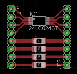
Figure 2: The circuit board used to test the Kapton tape solder mask concept consists of a TSSOP part, four resistors in a 1206 package, broken out onto headers.
The header pins rows are separated by 0.7” making them easy to install in a breadboard. The outline of the board is a square 0.9” on a side. I chose a combination of thru-hole and SMT components because the footprints are fundamentally different. SMT devices have both a tCream and tStop layer, while thru-hole components only have a tStop. This difference results in some extra steps in the following work flow. Finally, I selected the TSSOP packaged EEPROM because it’s the tightest pin pitch (0.65mm pitch with 0.23mm pin width) you can produce on the ProtoMat C60 PCB cutter. The resistors R1-R4 are standard 1206 packages.
Note I will refer to copper to which SMT devices are soldered as lands. The Kapton tape must be open over the lands and solder paste deposited in these areas. There are exactly 16 lands in Figure 1; the round holes for the thru-hole are not called lands, in part, because we will not be putting solder pates on them.
This is not a tutorial on creating a schematic and layout in EAGLE; it’s assumed that you have a completed layout like that shown in Figure 2. Once the layout is complete, you will be working with two tools in EAGLE, the Design Rule Checker (DRC) and the CAM post processor. We start with the DRC.
In order to create a solder mask for a board containing both SMT and thru-hole components, you must work with the tStop layer DRC and possibly the tCream layer. Let’s look at the simpler of the two first, the tStop layer.
In the lexicon of EAGLE CAD, the stop mask is what we are calling the solder mask. EAGLE CAD gives you the ability to make the stop mask larger using the Masks tab in Tools->DRC… as shown in Figure 3. Note that the figure shown on the left side (in this case a SMT pad and thru hole) depends on what cell is active. Unless there is some other need, set the Stop mask to be 0mil then the land or pad it’s over.
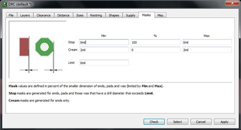
Figure 3: The stop mask settings for your design should set both Min and Max to 0mil.
Note, the longpads version of a header in the sparkfun library generates invalid output by the postprocessor (when exported as an encapsulated postscript file). This may not be an anomaly with this part, so make sure to verify that you have a valid solder mask before cutting your PCB. In my case, I was able to switch to a circular footprint and everything worked fine.
The following discussion on the tCream layer is only necessary if pullback for your SMT components is needed. If you don’t know what pullback is, then keep reading. During the cutting process, heat from the laser will eat into the borders of the cut making them larger then what you wanted. I will call this excess width kerf. Kerf is a problem because, with fine pitch components, the kerf from adjacent lands may eat away all the solder mask between the pins, causing the two lands will join together into one big open area. We can partially compensate for kerf, by making the holes in our solder mask smaller than their target size. I will call the amount by which the solder mask holes are reduced, the
Pullback of the mask. A 2mil pullback means the each edge of a solder mask hole are set 2mils inside the corresponding pad edge. You can control the pullback of the solder mask in the tCream layer using the Mask tab in Tools->DRC as shown in Figure 4. Note, you must do this in the tCream layer not the tStop layer, because you cannot make opening smaller in the tStop layer.
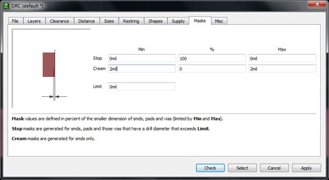
Figure 4: Manipulating the pullback requires changing the Min and Max values of the Cream layer. In this example the Cream mask has a pullback of 2mils.
As soon as you enter Cream values for Min and Max in and click on apply, the tCream layer in EAGLE will adjust itself to conform to this new rule. You should verify that this is working correctly by Displaying (View -> Display/hide layers…) layers 1 (Top) and 31 (tCream). Set the grid (View -> Grid…) to display a 1mil grid using lines. If you zoom in on any pad and you should see the tCream layer pulled back by 2mils from the edge of the Top copper layer as shown in Figure 5.
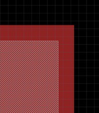
Figure 5: A tCream layer with 2mil pullback.
The amount of pullback needed depends on the material being cut. I’ve found Kapton tape to require almost no pullback, while painters tape for a disposable solder paste stencil requires up to 4 mills of pullback.
Now that we have our masks properly sized, we need to export them to Corel Draw. We start by exporting the tStop layer into an intermediate file format, encapsulated postscript (eps). To do this, open the CAM post processor (File -> CAM Processor…). Select EPS as the Device, file name and path (%N will give the output the same name as the file), and layers 20 and 29 as shown in Figure 6.
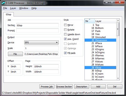
Figure 6: The DRC settings to export the tStop layer as an encapsulated postscript file.
Clicking “Process Job” will generate a file. You should repeat the process with layers 20 and 31 with a file extension tCream if you need pullback for your SMT lands.
Corel Draw
Import the tStop.eps file (File -> Import) generated by EAGLE into Corel Draw. Place in the drawing area. Make sure the properties toolbar is open (Edit -> Properties) on the right side of the window. You should see something similar to Figure 7.

Figure 7: Raw tStop layer in CorelDraw.
Select everything (Crtl-A). Using the Fill tab (bucket icon) in Object Properties, select Uniform Fill from the pull-down and select white as the fill color. In the outline tab (fountain pen icon) select hairline width and red. This should result in an image like the following. Note that it might be a good idea to stretch the outline of the solder mask outwards by 63 mils on each side so the mask can be folded down to cover the edges and add additional coverage to the edges of the board.
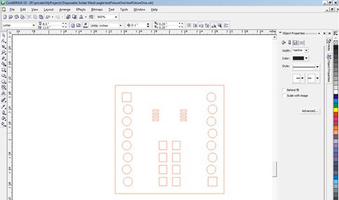
Figure 8: Edited tStop layer ready for the laser cutter. Stop here if you don’t need pullback.
The following instructions are needed if you are importing the tCream layer. You will need to edit the tStop layer. Start by ungroup the object by first selecting all the objects (Crtl-A), and ungroup (Arrange -> Ungroup All). You can now select individual elements and delete them or lasso groups of elements and delete them in bulk. Now import the tCream layer, convert all the fill to white and the lines to read hairline (just like the tStop layer).
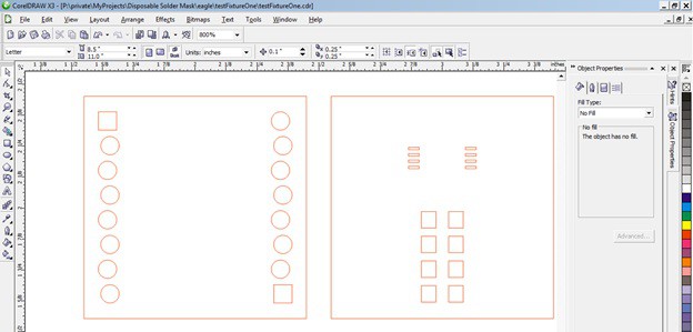
Figure 9: The edited tStop (left) and tCream (right) layers ready to be merged.
Select all the objects in the tCream layer by lassoing the square. Click on the upper left corner of the square outline and drag the tCream layer until its outline snaps to the tStop layer. The result should look like Figure 8, only with slightly smaller openings for the SMT lands. You may want to delete one of the outlines as the laser cutter will make a second, unnecessary, pass along the border of the solder mask.
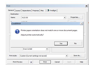
With out setup, all you have to do is print the image in Figure 8 in Corel Draw using File -> Print. When you do this you may get the following pop-up message from CorelDRAW. You must answer No in order to get proper print output.
Universal Laser VLS 3.50
This final step of the mask process is dependent on which laser cutter you are using. Regardless, of the type, you will have the ability to fine tune the laser strength to get acceptable results.
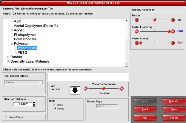
I started by placing the Kapton Tape on a backing board. After some experimentation, we settled on the following parameters:
- Material: Plastic -> Polyester -> MylarTM Film
- Thickness 0.01”
- Red Vector Cutting -50%
- Blue Vector Marking +50%
- Experimental results
A series of solder mask was created using process described in Figure 9 and is shown in Figure 10. Accordingly, each mask had a specific amount of pullback from 0mils to 5mils. The first experiment (at left) were performed with 0 mil pullback and aimed to determine the Red Vector Cutting power. The goal was to have just enough power to reliably cut through the tape. The choice between Full power and -50% power was easy to make as -50% cut through the tape. At this lower power setting, progressively larger pullbacks were cut. The goal was to have the open windows in the TSSOP lands be exactly the same width as the pads while still preserving the mask between the pads.
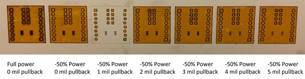
Figure 10: A series of solder mask created to test process parameters for Kapton tape. The solder mask with -50% power and 1mil of pullback was used for the board shown in Figure 1.
After close examination of the mask under our binocular microscope, I decided to put the 1 mil pullback mask on the raw PCB. The results in Figure 1 look pretty good with the most serious error being the lifted up lower left corner where the solder mask was removed from the back material shown in Figure 10. Note, that this problem could be mitigated by increasing the dimension of the mask by 63 mils. Increasing the size of the mask would allow you to limit damage to the mask (inevitable when the mask is removed from the backing material) to an area not actually used to cover the surface of the PCB. To get a better idea of the alignment of the land windows, I took a picture under 10 x magnifications through our binocular microscope. Figure 11 shows the mask aligns almost perfectly.
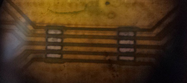
Figure 11: A close-up of the cuts made for the TSSPO part using 1mil pullback on the SMT lands.
The final test was to apply solder paste to the board, drop on some components and see how the board reflows with the Kapton tape. We have been using the hot plate skillet reflow technique to reflow our PCBs for 6 years with a great deal of success, so this was the process used for this test. Figure 12 shows the test board, before and after reflow.
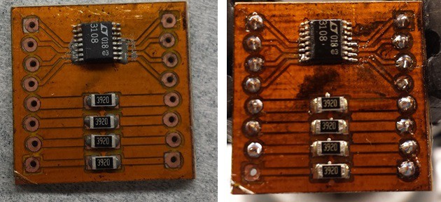
Figure 12: The board with Kapton-tape solder mask before (left) and after (right) reflow soldering on a skillet and attachment of the header pins.
I placed a liberal amount of solder flux on the header pin pads before soldering the headers in. This in addition to the flux in the solder paste motivated me to place the finished board in our ultrasonic cleaner for 15 minutes. The completed and clean board is shown in Figure 13. Neither the reflow process nor ultrasonic cleaning significantly changed the appearance or adhesion of the Kapton tape. With the exception of the solder bridge on the left side of the LTC3108 (I did not have any solder wick), the board turned out great, surpassing expectations
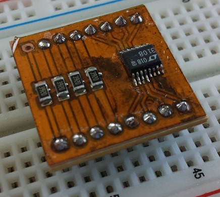
Figure 13: Completed and cleaned circuit board - Kapton-tape solder mask success!
References
Kapton tape
KAPTON ALTERNATIVE POLYIMIDE TAPE 1 MIL (70000)
SKU: 70000-0200-001-36-AM
ProtoMat C60 PCB Cutter
http://www.lpkfusa.com/RapidPCB/CircuitboardPlotters/c60.htm
Universal Laser VLS 3.50
http://www.ulsinc.com/products/vls350/
Reflow Skillet Technique
https://www.sparkfun.com/tutorials/59
Branson 1800 Ultrasonic Cleaner