 Yann Guidon / YGDES
You will find a lot of background information in #AMBAP: A Modest Bitslice Architecture Proposal and #YGREC16 - YG's 16bits Relay Electric Computer, this new project contains the latest developments since April 1st.
Logs:
1. Evolution of the architecture
2. DRAM (again)
3. PROM boards
4. Assembler and disassembler
5. I hope that's enough
6. First DRAM array prototype
7. The Program Counter's circuit
8. Tubular bell
9. Flip Dots !
10. Electromechanical User Interface : the Assembler board
11. How to drive РЭС15 relays with a computer ?
12. Programming the YGREC
13. Carry chain considerations
14. I hope that's enough this time
15. The instruction register (cont'd)
16. Now it should be enough
17. I can see now
18. Instruction display panel
19. Relay DAC
20. Display technology again
21. Chime on me...
22. DIY backplane construction
23. Yet another fork
24. ...
Let's build a computer. Literally a bare metal computer, that is also funny and ridiculous !
- Ridiculously slow (20 IPS ?)
- Ridiculously greedy ( >200W)
- Ridiculously noisy (OK, that's actually desirable)
- Ridiculously incompatible (it's a brand new architecture called YGREC that I develop at the same time)
- Ridiculously limited (512 words of DRAM, a bit more instructions)
- Ridiculously unreliable (I added 2 parity bits)
- Ridiculously useless (except to compute the Game of Life to prove my point that ridicule doesn't kill)...
It started almost as a joke one year ago with #SPDT16: 16-bits arithmetic unit with relays but the joke was on me and the fun, the learning, the charting of new design spaces have slowly changed my approach to computer design.
Now I have a complete architecture, an instruction set, all the needed essential parts, and I continue to put things together in the logs. In parallel, every new breakthrough is reinjected in such projects as #YASEP Yet Another Small Embedded Processor and #F-CPU (which was rebooted thanks to this project).
The YGREC architecture is pretty simple and designed to use as few resources as possible, yet run the #Game of Life bit-parallel algorithm efficiently (though it's not the original goal or purpose, there was none in fact, it was just "loooook those cute relays must be fun to use!")
The datapath is shown below : The 16 registers (including PC) are accessed as the SRCX operand while only 8 registers are read as the SRC operand (because such a large MUX uses a LOT of relays). The narrower SRC operand can be shifted/rotated, or substituted with an immediate value from the opcode. Both operands are then processed in the ALU (either in ROP2 mode, where all combinations are possible, or in Add/Sub mode where comparison, carry and Min/Max are possible). The result is checked for being zeroed, and sent back to the register set.
Really, it can't be smaller or simpler while preserving functionality (I'm not doing a Brainfuck computer, I'm interested in actual practical architectures)
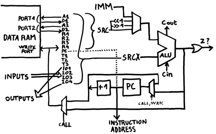
The register set maps memory addresses, memory data, the Program Counter and Input/Output ports. Only R1-R4 and T1-T3 are "standard registers", making the YGREC a hybrid architecture: it looks like some classic RISC and also behaves like TTA (for operations other than Shift/ALU/ROP2). There is indeed no actual opcode, only 32 combinations for the ALU and 16 Shift/Rotate combinations to care about. The architecture is highly orthogonal, all the essential operations can be achieved with a combination of the available fields and special registers. All the instructions are predicated, except CALL which replaces the condition "NEVER". In this case, the result goes to PC, while PC+1 goes to the register set.
The YGREC can be reduced to MUXes and DFF registers (which can also be made with MUXes). This maps perfectly to dual-throw relays !
Some characteristics (if you haven't read the other project) :
- Based on a bitslice architecture, with 18 bitplanes (16 data bits and 2 parity bits, one bit per byte)
- Uses about 3000 РЭС15 relays (low voltage, circa 1989), a ton of diodes (but not for the logic), 10K capacitors for the dynamic RAM and CCPBRL
- 24-bits wide RISC instructions with predicates
- integrated debugger and assembler/disassembler "electromechanical UI"
- multiple power rails (3.3V, 6.6V, 12V, 24V) to reduce currents with long strings of relay coils (a consequence of using CCPBRL)
- Separate Execution and Control assemblies (I have focused mainly on the execution part but the newly defined instruction format makes it easy now to design the control side)
Some innovations or discoveries were made since the project started:
- CCPBRL is a different way to use relays in hysteretic mode, with significant advantages over the usual on-off methods (Vcc-GND or Vcc-open). Who would have imagined that today, it's possible to invent new circuits with such an old technology?
- A "lateral" computation algorithm for the Game of Life (I stumbled on this when I wanted the machine to do "useful work" that would appeal to everybody while showing off the performance and the peripherals)
- Balanced command binary trees are a direct consequence of CCPBRL's specific requirements but can be directly reused in ASIC and FPGA to manage propagation delays and reduce the number of high-fanout signals
- Diode-relay carry chain (derived from @Tony Robinson's idea)
And I'm not even mentioning the creation of a complete new ISA from the relay up.
Thought of the day:
Usually, one prototypes a circuit in FPGA before implementing it in other technologies. Here, I seem to do the reverse :-D
This project also taught me an important historical lesson : electricity-based computers could be made without transistors, but they are insanely hard without diodes. Diodes are what made computers practically possible, during the last century, and they needed to become reliable enough and cheap enough to be deployed en masse, paving the way for the transistors...
Without diodes, the AMBAP's memory systems couldn't work (1 diode per bit for the instruction PROM, 2 diodes for the DRAM). The input panel couldn't work either. The logic/datapath can work without but benefits from good diodes, and it would not have anywhere to store the vast informations it needs to process, thus reducing it to a dumb FSM...
This assertion is confirmed by the #Hot logic project.