 Eric Hertz
I've mentioned this a few times in past logs, using resistors to route data-flow where otherwise it would be "logical" to use logic (gates, buffers). Especially to interface with the *bus*. A few reasons: adding buffers requires the addition of another control-signal for each device connected to the bus, resistors are cheaper than buffers, and of course I'm attempting to use the SDRAM's inherent features wherever possible... Maybe not *great* reasons, probably not ideal in a *product*, but maybe easier in some cases for hobbiests, etc., and just another way of looking at things...
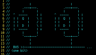
(Of course, the DQ-latches have an Output-Enable, which gets toggled as-appropriate).
So, a little bit of math might suggest that this would be quite difficult, especially when connecting *multiple* devices to the bus. The input-capacitances of all those devices (and the processor's bus, itself) add up...
E.G. at 133MHz, say, 3ns is a reasonable rise/fall time... And say the capacitance of the inputs is something like 50pF... T=RC... that'd be 60ohms for our resistors. Yeah, that'd be tough... lotsa milliamps when several DQ-latches are holding a "1" and the bus drives the latch-inputs to "0". Etc. Etc. (OTOH: In most of these cases, there's no reason to drive the outputs at the same time as there's data on the bus... hmmmmmm)
------
One big consideration is the fact that the bus is generally *not* going to be 133MHz.
(Pi's GPIO toggle rates allegedly max out at around 50MHz, and the step-wise process of controlling the bus is several steps between each read/write).
So, we might be able to bump those resistor-values up a bit without dramatically slowing *bus* transactions.
Here's some data from the Micron 64Mb SDRAM Datasheet:
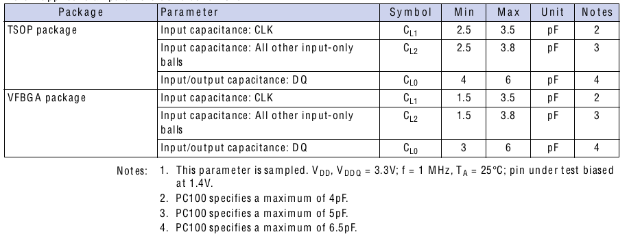
But, this shizzle adds-up, right? Each DIMM may contain up to *16* chips (8 per side) all connected to the same command/address lines... That's 16*5=80pF! But, also, the Command/Address pins are directly-wired to DQ's, so that's 86.5pF, then the output of the DQ-latch...
And that's on the *non-bus* side of things... (is this going to affect free-running?)
Output-High and Output-Low voltages are spec'd at 4mA, too... (but not listed as a PC100 spec). so, hmm...
So, not sure... There may be some more in-depth pondering to do as we bump up this thing's speed...
----------
This might be turning into two separate paths...
One that can be built with a minimum of parts, on a breadboard, etc... and maxes out at a low-speed (30MS/s, currently), depending on your available parts... That's still greatly-functional for many people's needs, especially for something that could be assembled in a weekend from parts-at-hand.
The other, to achieve 133MS/s, might require more and higher-quality parts; buffers (maybe latches?) in the feedback-path, buffers instead of resistors in the bus-interface and other locations, an additional 8-bit latch for the bus-buffers' output-enables... Probably a couple extra 8bit latches, as the "address-jumping" technique wouldn't then make sense to implement... And, of course, would need to be on a PCB.
At this point, the second path seems a long ways off, if at all. There's still a lot to be seen regarding just how much can be pushed outta solderless-breadboarding, etc.
Discussions
Become a Hackaday.io Member
Create an account to leave a comment. Already have an account? Log In.