 Eric Hertz
UPDATE: Apparently I've found a general-spec... See the bottom
-------
sdramThingZero is still on-hold, but of course still runs 'round the ol' back of the head... There's nothing really stopping progress, just haven't gotten around to designing/ordering PCBs. In fact, the breadboarded sdramThingZero is still sitting on my desk right under my monitors.
------
So here's something interesting:
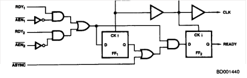
Does that look familiar, at all?
Yep, it's pretty much exactly the same topology as the "one-shot" logic used in this project. Two flip-flops in series, both receiving (in some form) the input, performing some logic on the original and the delayed/latched output, and even an async-input (similar to my "one-shot Bypass" input). This is from the Intel 8284 datasheet, that's the clock-generator used for PC/XT (8088) computers. Besides clock-generation, the 8284's other key feature is what we see here, synchronizing an asynchronous "READY" signal to the system-clock... Just like my one-shots synchronize an asynchronous Chip-Select or Clock-Enable signal to the SDRAM's clock.
Why's this interesting to me...? Maybe this is some sort of de-facto topology used all the time...? The fact is, I designed that circuit without having looked it up... I used knowledge of what was going in and expectations of what I wanted out, and I designed a circuit to do-so. I knew it *would* work, for the most-part (what happens if the asynchronous input comes between the setup/hold times? TI's thoughts here), but I didn't expect that it was good 'nough for a product. And yet, there it is!
------------
SDRAM initialization:
Note, first, I'm no trained expert... this is all what I've gathered in my experience with hacking SDRAMs... (single-data-rate, NOT dual-data-rate!)
See also: https://sites.google.com/site/geekattempts/home-1/sdramthing/using-sdram
Someone commented on my youtube-video, prompting me to respond that... basically... the SDRAM initialization-process, unfortunately, pretty much requires the entirety of the functions one might need to make use of the SDRAM, including ones that are otherwise unnecessary, and more.
What do I mean...?
Well, it's not like SRAM, where you can just turn it on, write a byte, and read it back (and you can repeat the write/read process at any other address, immediately thereafter).
It's not like DRAM, where you can just turn it on, select a row-address, write a byte, and read it back (and you can repeat the select-row/write/read process at any other row/col-address the next time 'round).
So what's it like...?
Well, first, let's *merely* look at the write/read procedure.
Note that this example differs from the SRAM/DRAM examples given earlier in that this can only happen *after* initialization, it can't be done immediately after power-up (we'll come back to that).
To write a location and read-back you have to open a row (similar to DRAM), then you have to perform a write at your column, then you can read it back... That's pretty much the same as DRAM, except that if you want to do-so again at a different row, you have to explicitly choose to *close* the original row, first. (Closing a row is called "precharging").
So, realistically the write/read-back procedure is similar to DRAM *unless* you want to access another row.
But, we're just trying to do the *simplest* experiment, right...? Just to make sure we're wired-up correctly.
(See Note1 below)
Then you'd be set, you'd never have to think about precharging. (And, another cool side-effect is that as long as a row is open, it is inherently stored in registers rather than merely dynamic-RAM cells/leaky-capacitors, so needn't be refreshed... Handy!). BUT, you *would* have to consider the fact that you can't "activate" a row when a row's already active. Which means your write/read/repeat procedure needs to be: open/activate, write, read, write, read, write, read... (don't open/activate a/the row each time!)
So, now...
Why this long explanation, we were talking about initialization.
OK, SRAM: write/read, write/read...
DRAM: open-row, write/read, [optionally open another row], write/read...
SDRAM: open-row, write/read [optionally: close row, open another row], write/read, write/read...
But, again, we're trying to do a *really* simple experiment... so let's skip the optionals... We'll do *everything* in the same row... then we don't need to implement the "close-row" ("precharge") procedure...
So, to do a *really simple* experiment, we only need to implement three functions, right? open-row, write, read. (And, if we were implementing auto-precharge, as in Note1, we could access the entirety of the memory, and perform additional functions like refreshing, with only those three commands!)
Nope.
Because, unlike SRAM and DRAM we also have to initialize the stupid thing.
Because it's a state-machine, which doesn't power-up into a known state. It has a configuration-register, which (per-specs) isn't automatically-initialized to a known/valid value on power-up... and, should one manufacturer's model just happen to power up in one of *many* of the possible valid states, in the majority of cases, it won't be usable with a *really simple* system.
So, now, we managed to figure out how to whittle down the necessary commands to *use* the memory down to pretty much the same as DRAM: open-row ("activate"), write column, read column (with auto-precharge).
But, the initialization-procedure, which you'd be lucky to get the system working without, includes many of the commands we managed to avoid... Including: "Precharge All" and "Auto-Refresh", in addition to the obviously-needed "Load Mode-Register" (configuration-register) command.
So, to *reliably* use the system, even just for quick verification you understand its wiring/functionality, you have to implement *numerous* commands, many of which will never be used again, and all of which result in no feedback whatsoever as to whether they actually worked... until it comes time to write/read. A whole lot has to be implemented "blindly."
To top that off, many of these commands *cannot* be executed repeatedly (as would be the case if your "chip-select" signal is active for longer than *exactly* one clock-cycle). Which is why I use one-shot circuitry, in this project, and why other earlier versions of sdramThing use inline-assembly to strobe the chip-select for exactly one clock cycle... and why SDRAM *cannot* (within specs) be interfaced to GPIOs, without one-shots, in systems where exact clock-cycle-counts can't be controlled/predicted (e.g. GPIOs on a Raspberry Pi, or any system running interrupts, an operating-system, or with cache, branch-prediction, unpredictable wait-states, etc.)
WEEE!!!
-----------
Note1: Technically, it looks like it might be possible, within specs, to simplify the write/read/repeat process to be more like DRAM, wherein the entirety of the RAM, including other rows, could be accessed with a open-row/write/read (and no need for an explicit close-row command). You can perform the "read" (following the "write") with an "auto-precharge" by merely changing one bit during the "read" command. Then, you could run the same procedure as with DRAM: select a row-address, write a byte, and read it back (with auto-precharge), repeat anywhere you like. The problem is that, because it's *synchronous*, doing it this way is even more complicated than adding an explicit "precharge" command, because it requires that you know *exactly* the number of clock-cycles between requesting the "read-with-auto-precharge" and actually *reading in* that data into your processor, etc.
----------
So, I've been contemplating whether the process of just getting started could be simplified a bit... (while still being reliable enough for early experimentation). And, looking into a couple different specifications from different manufacturers, it looks like the answer is "not really".
The problem is, *in general* the specifications are pretty clear, in their lack of clarity regarding what's to be expected of/from these devices, in general.
E.G. the Micron datasheet I've been doing all my development from explicitly states that it's acceptable to interrupt a read-with-auto-precharge with another read in the same row. Handy. So then you could *always* request an auto-precharge, and if you want to, you could hold that "chip-select" line as long as you want (even long-after reading in the data), and the result would be multiple back-to-back "read" commands, at the same memory-location, each interrupting the auto-precharge of the previous... And, essentially, once you eventually get around to releasing that Chip-Select, the auto-precharge would occur. NICE! The Micron datasheet even shows timing-diagrams of this interruption. It's a thing!
Now, I've just dug up a new-to-me Hynix datasheet which explicitly states that interrupting a read-with-precharge with another read (or write) is *not* allowed. In fact, the wording is "ILLEGAL".
--------
So, what's the point...? I guess it's a question of whether you want to work within the *clearly-defined* specifications for generic devices--not relying on specifications which are vague or device-specific--in which case you should be able to wire-up any brand of chip and use the same code... Vs. whether you want to work with a specific chip (and gain the benefits of its additional features!)...
Note that PCs (Computers) have some sort of general specification that works with darn-near all conforming devices that might be thrown at 'em... So, there must be some specification, somewhere (jedec? paywall?) that defines the guarantee-ables that all devices conform to.
In my experience, I've been referring to that Micron datasheet almost [but-not] exclusively, and expecting that where it's unclear, it's probably that way due to unclarities in the general-spec (e.g. can you perform a row-activate after a row-activate, without an intermediate precharge, if they two row-activates occur *in the same row*? What happens when you select a burst-length that's "Reserved"?)...
It would be a mistake, (one I've probably made) to interpret any specific device's datasheet's specs as *general specs* for all devices conforming to the PC-66/PC-100/PC-133 specs. (E.G. the Hynix device lists burst-modes of up to 128 columns (aside from "full page" bursts), whereas the Micron only lists up to 8... the other mode-settings being "Reserved." E.G.2: Can CKE be disabled at any time, especially in the middle of an operation, or only during burst-reads/writes?)
I haven't found the all-encompassing "general spec" used by PC-66/100/133 *devices*. But, so far, I don't think I've made use of any device-specific features, and have been testing my code on DIMMs from several manufacturers.
And, again, if you're planning to work with a *specific* device, then these factors don't matter... use what the datasheet provides, or experiment and see what happens! Just keep in mind that if you try to do writes/reads without doing an initialization, first, you may not get *anything*, or may get *really confusing* results that work sometimes and not others.
----------------
So, come on... I've been working on sdramThing for nearly five years, now... between sdramThing1.0 and 4.5, and now sdramThingZero. So all it takes, this time, to find an alleged general-spec is a search for "PC-133," a click-through to the wikipedia page, and opening the very first reference? Please, you think I haven't done this before?
Here's the great bit:
The objective of this document is to define a new Synchronous DRAM specification (“PC SDRAM”) which will remove extra functionality from the current JEDEC standard SDRAM specification, so that it will be a “fully compatible” device among all vendor designed parts. It should be easy to design and manufacture and highly cost optimized for the main stream volume desktop Intel architecture PCs.
Right... So, assuming most manufacturers of PC66/100/133 SDRAMs want to be compatible with Intel-Architecture PCs... they'd probably meet all these specs... which is exactly what I was talking about. WEEEEE!!!!
(First observation: Burst-lengths of greater than FOUR are "Reserved". And Full-Page bursts are as well?! WTF. I never...
Discussions
Become a Hackaday.io Member
Create an account to leave a comment. Already have an account? Log In.