rolmie
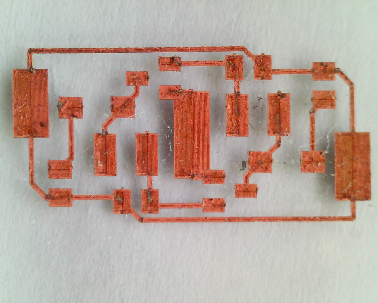
The goal is to make hardware prototyping easier by providing a middle ground between dealing with either developer and etching chemicals, loud mills or long shipping times from china. Ideally a medium dense single layer 4x4" PCB for SMD components can be manufactured in less than an hour with little to no attention.
Status Quo:
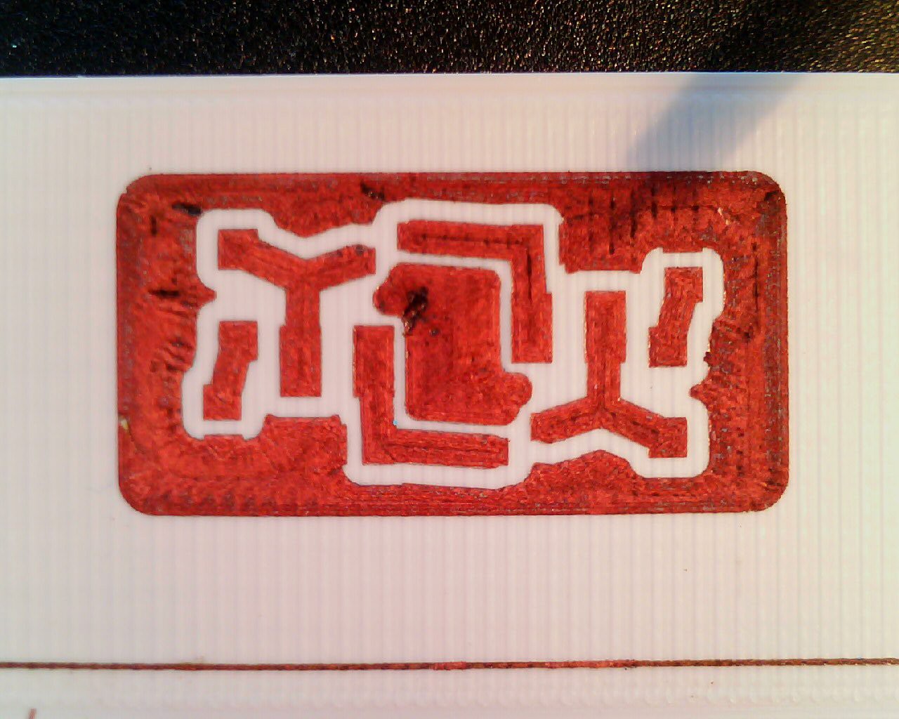
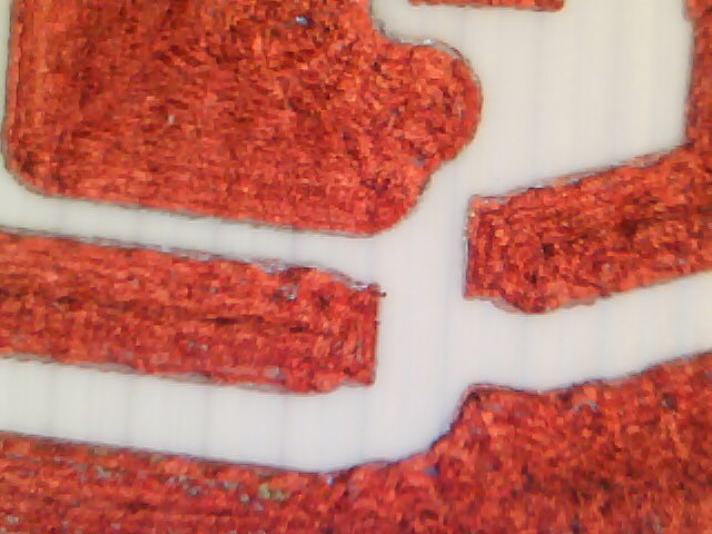
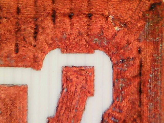
"Printing" a single layer of copper on a PET-G works and conductivity 2-3 orders of magnitude better than conductive plastic, but 1-2 orders of magnitude below that of solid copper, is achievable.
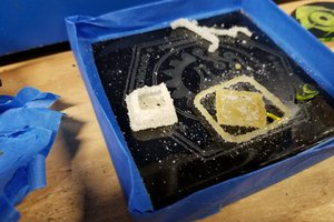
Component mounting still needs to be solved, low temp solder seems to promising, alternatively conductive epoxy.
Chemistry:
Copper(II) format preparation
I mixed 12g Copper carbonate with 126ml of DI water and 10ml of 75% Formic acid in a glass jar. The reaction is slow and takes a few hours at room temperature. CO2 is released during this process, do NOT close the jar tightly. Use the usual safety gear (googles, gloves) and keep the room ventilated.
Laser:
I'm using a 900mW 405nm laser diode, probably extracted from a Pioneer BDR-209 BR recorder. The driver limites the current to 200mA (about 300mW power) and PWM is used to limit the power further while printing.
450nm seems to work as well, but requires significantly more power, it might be difficult to use on heat sensitive substrates. I stooped using it once I had a 405nm laser available.
Substrates:
- Glass (microscope slides): very easy to work with, can't be destroyed by the laser. Adhesion is limited.
- Polyimide (on glass): somewhat sensitive to power. Better adhesion than glass.
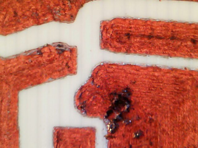
- Fiber reinforced epoxy (FR4): sensitive to power, easy to burn. Difficult to wet, sanding the surfaces helps but exposes porosetiy.
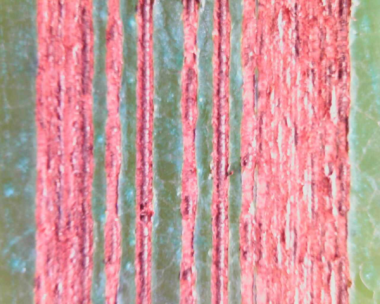
- white PET-G: very sensitive to power. Easy to wet with window cleaner. Quality traces and conductivity achievable with multiple layers (3 typical)
- black PLA: didn't work, maybe because black
- TPU (flexible): didn't work
Sample preparation:
I'm using a syringe to apply small quantities of saturated Copper(II) format solution about (0.1ml - 0.5ml per square inch). Usually a wetting agent is needed to overcome the surface tension. Dishwasher detergent works quite well, alternatively window cleaner as it contains ethanol, particularly good with PET-G. The samples are usually dried with the heated bed set to 75°C.
Power Control:
I'm using Repetier Firmware, but not in Laser mode as it only allows a fixed PWM uncoordinated to the actual gantry. Instead I'm using the E parameter of the G1 command to control the energy that is applied to each segment. The principal is fairly simple, the E axis is set to 15625 steps per mm with a maximum speed of 1mm/s. A Arduino Nano is used to broaden the step pulse to 64µs (1/15625). This creates a PWM signal coordinated to the actual gantry speed.
ToDo's:
- Component mounting is unsolved. PET-G might actually work with Tin Bismuth solder (138°C)
- System (pump/needle) to apply the liquid precursor selectively only where needed
- Better integration with 3D printing, e.g. multiple layers, add features to help with component placement

 FabLab München
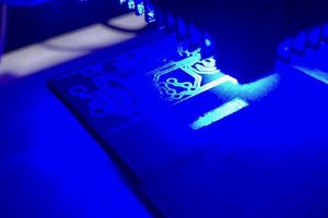
 igorfonseca83
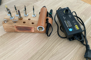
 vincentmakes