 Raul Funes
Ok, so having already prototyped the circuit to make sure it works as expected, I can move on to designing the printed circuit board. For this task as I commented on my previous blog, I will use Eagle CAD 7.5 which can be downloaded here Eagle CAD.
I believe using Eagle rather than Altium will help to make this project more accessible since it cost nothing as well as has a more friendly interface or so I was told. However the use of this software is completely new to me, so It´s very likely that I make mistakes whilst getting the hang of it, I will try to keep them on the log, so you can learn from them and save yourselves a good deal of pain...
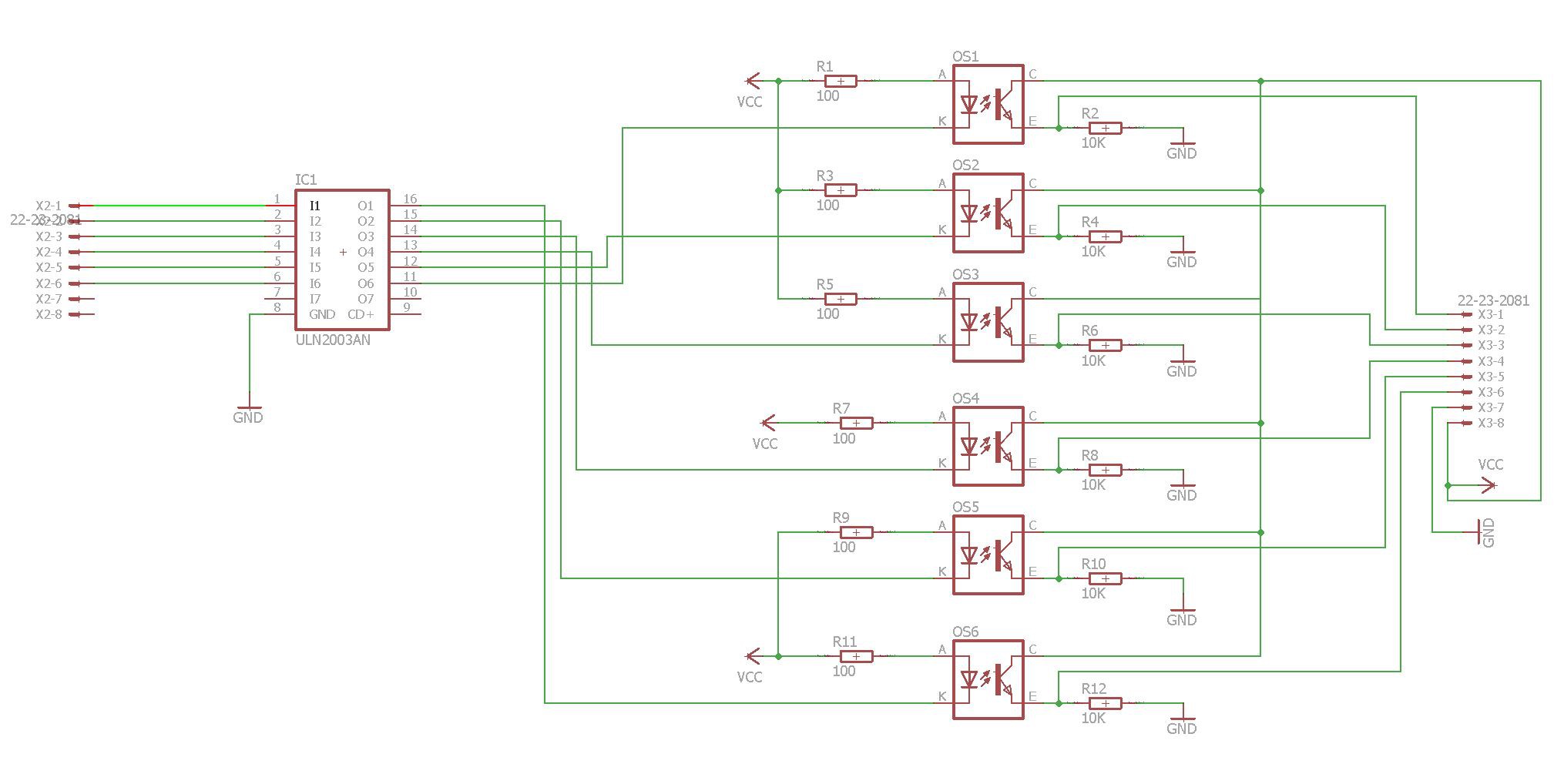
ok so designing a pcb on Eagle as far as I´ve learned consists of two parts, designing the electrical circuit, and then transfer the design to the physical layout of the board.
Because of my previous exposure to software like Multisim from National Instruments, I found the schematic part quiet straightforward, having all the options you probably need for this design on the taskbar on the left side of the screen.

when it came to build the circuit, I found a very attractive feature of eagle, which is the amount of libraries available online for pretty much any component you might want for your circuit. For this circuit I needed the Tcrt-5000 sensor library file, it did not take me long to find it online and download it. I have upload the library which can be found on the files for this project. Once I had the file downloaded, I copied it into the lbr folder located at Eagle V7.5 folder at the C drive.
Once the file is located in the libraries folder, I opened eagle, open my schematic, select library at the top task bar, update, and select those files I wanted to update, in my case it was the tcrt-5000 sensor.
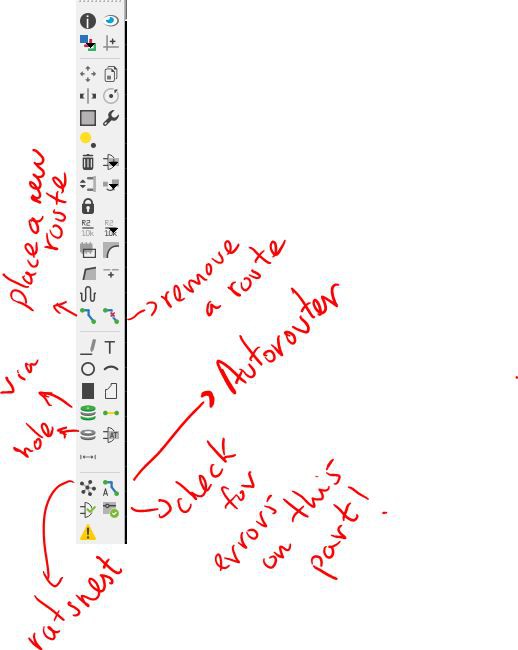
once I had the components I needed , I carried on with designing the schematic circuit, as I said previously I found building it quite straight forward. Once I had the circuit done I found out a very useful tool of eagle, which is the ERC function, This command is used to test schematics for electrical errors and I strongly advise you to use it, in my case I did not know at first that even existed so as soon as I was done with the schematic I moved on to create the board, it took me a while to figure out why some electrical connections were missing on the physical layout. this command lets you know where the problem is.
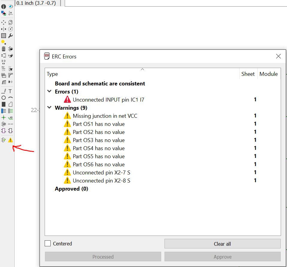
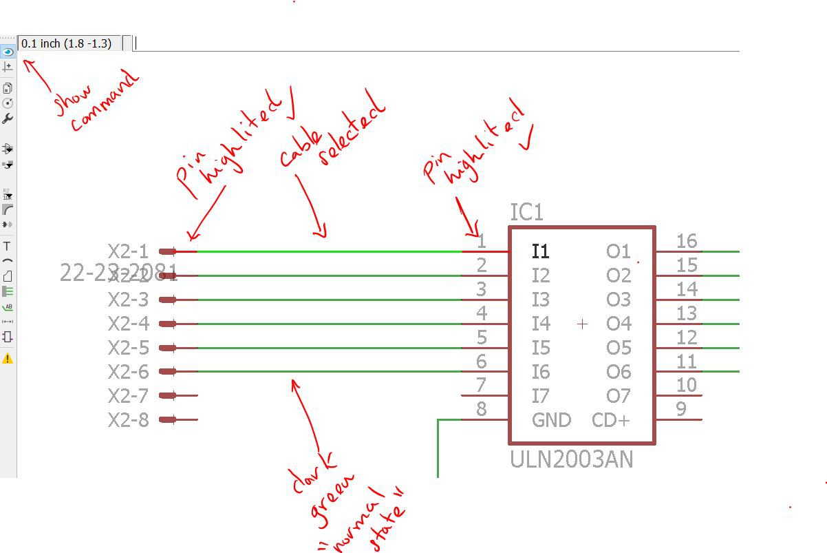
this tool gave me some errors that at first I thought they were fine, at first glance the connections seemed to be properly done, once again I learned a powerful tool from Eagle which rescued me from the problem! The command is named show and what it does it lights any connection you touch allowing you to see whether the connection is made from the beginning of a component to the end of the component the wire is supposed to join. if the pins of the components do not light something is wrong and most likely you will have to rewire it!
 once I fixed those faulty connections my schematic was ready, so I moved on to the layout of the board part
A couple of tips from my personal experience: The main advise i was given when populating the PCB before routing was: " make sure you wires don´t cross each other" so based on this You might have to come back to the schematic circuit to make slight changes which might look a bit more "messy" on the electrical schematic, but makes the populating of the PCB far easier and reduces the crosses between wires.
the last advise is a very personal one, but since it made it more difficult than it should have for me, I thought I would share it anyway. My background as well as big part of my degree is electrical so we have a strong habit of associating red with power (+5v,+3.3V etc) and blue or black with ground (0V) so when I was routing the PCB, almost unconsciously I was aiming to use the top layer (Red wires) as the ones carrying the voltage, and the bottom layer(Blue wires) as the one carrying the GND. Needless to say this made the routing more challenging and the PCB bigger as well. Luckily I realised on time that as stupid as it sounds Colours are just colours!!!! so by using the two layers better, routing became easier and faster. The PCB also reduced in size!
 I´ll keep you posted!!!
Discussions
Become a Hackaday.io Member
Create an account to leave a comment. Already have an account? Log In.
hi
I'm a 2nd electrical engineering student building a line following robot using trct5000 and lm741 to amplify the signal. is it possible for you to send me the file for the pcb so I can make it and add amplifier in.
thanks
Are you sure? yes | no