 Reed Foster
(I will be updating this at https://github.com/reed-foster/uCPUvhdl/wiki and eventually will remove this section)
Designing a CPU:
In this section, I will describe how the muCPU was designed and how it works. Any blocks of text in italics is information to explain why I made a certain decision; it does not need to be read to understand how the muCPU works.
Step One: Instruction Set
When designing a CPU, the first thing to consider is what features/capabilities you want it to support. There are two main design philosophies when it comes to designing instructions for an architecture. Originally, when computers first emerged, memory was very expensive, so data and instruction widths were kept to a minimum in order to reduce cost. In addition, processors supported a wide variety of simple to complex instructions; they supported memory addressing for arithmetic operations, and some instructions executed multiple steps. Programmers used a small amount of complex instructions to minimize memory usage. However, with technological advancements and shrinking transistor sizes, manufacturers could fit more and more transistors onto integrated circuits, improving the storage capacity and processing power of computers. With an increase in storage capacity, programmers didn't have to worry as much about how many bytes their code took up; instead, they could focus on the speed of their code. With this increase of memory came the second design philosophy known as RISC, for Reduced Instruction Set Computing (while the previously mentioned design philosophy came to be known as CISC, or Complex Instruction Set Computing) . RISC processors are designed based on the idea of executing many very simple instructions very quickly, rather than a few complex instructions that each take a while to execute. Since CISC style processors are inherently more complicated to design, often times with multiple instruction bit widths and very complicated decoding circuitry, I decided to base the muCPU design off of a very simple (in some aspects) RISC style instruction set: MIPS. The MIPS Instruction Set consists of three types of operations: r-type, i-type, and j-type. As one might suspect, the "r" in r-type is for register, while the "i" and "j" in i-type and j-type are for immediate and jump.
MIPS is a load-store architecture (meaning that memory is only accessed through load and store operations; arithmetic is done with a register file, a small bank of very fast memory) implemented with a pipeline, in fact, its name used to stand for Microprocessor without Interlocked Pipeline Stages. This basically means that each section of the pipeline takes one clock cycle to execute. MIPS uses a classic five-stage RISC pipeline consisting of the following stages: Instruction Fetch, Instruction Decode (and usually operand fetch), Execute, Memory Access, and Write Back. One of the problems with pipelining is that it introduces situations known as hazards. Hazards include structural, data, and branch hazards. Structural hazards are usually eliminated fairly easily; insert another adder here or there and usually all structural hazards are eliminated. Sometimes more complicated methods (such as register renaming) are required. Data hazards can occur when an instruction operates on data that has not yet been written back to the register file. Here's an example:
lb r2, 126(r5) ;load byte located in memory location (126 + contents of r5) into r2
add r2, r3, r4 ;add r3 and r4, storing the result in r2
The first instruction loads a byte from memory into r2, however, it takes 5 clock cycles for the instruction to be completed, so the second instruction will use an old value in r2, which is not what the programmer expects. One of the methods to negate this hazard is forwarding, a strategy that I used in my 32 bit MIPS CPU. In my implementation for that project, I save a small list of values and their corresponding register addresses that they are intended for. This list is located in the execution stage of the pipeline, and when operands arrive from the decode stage, they are compared with the list and replaced with an updated value if necessary.
Finally, there are branch hazards. Branch hazards occur any time that a conditional branch instruction is fetched. When the next instruction is fetched, should it be from the address if the branch is taken, or from the next incremental address. To give the processor a little bit of time to make this decision, the MIPS architecture executes every instruction in the slot after the branch instruction, the branch-delay slot. Next, the outcome of the branch is predicted, and the branch instruction is speculatively executed, meaning that the next instruction that is fetched could be wrong. By the time the original branch instruction is actually executed, only one potentially incorrect instruction has been fetched, so the performance hit is minimal if an incorrect prediction is made; about the same as if the pipeline were stalled until the outcome of the branch instruction was determined. If the branch is predicted correctly, then hey, that's great.
All right, back to the project. Since this my first CPU design on an FPGA, I wanted to keep it simple. Instead of a 5-stage pipeline, the muCPU has 2-stages, which also conveniently eliminates both data and branch hazards (because it still executes the instruction after the branch). This is not the only change to the MIPS design that I made. Instead of 32 bits for an instruction, the muCPU uses 16. In addition, each pipeline stage takes four clock cycles to execute, and the first stage idles for most of the third and all of the fourth clock cycle (shame on me for bad pipelining). Finally, since the muCPU instruction width is half the length of that of MIPS, the muCPU register file is much smaller, and the instructions are not binary compatible (duh). I guess with all of these changes, the final design that I have produced is a far cry from MIPS, but the original intent was to produce something fairly similar.
I've chosen to only implement the first two instruction types because with an 8 bit processor, the additional immediate bits that the j-type instruction provides are useless; I only need an 8-bit immediate, not 26 (the jmp address bit width). As such, I use the bez with the operand r0 (register0 is hardwired to 0) as an "unconditional" branch. Unfortunately, it is not exactly the same as the jmp instruction; instead of setting the program counter to the specified jump address, a bez r0 increments (or decrements) the program counter by the specified address.
Below I have included a table of the bit pattern for each two-byte (16-bit) instruction that the muCPU processor supports. The bottom row of the table shows the bit ranges for each component of the instruction (for example, the first field (the opcode) is two bits; bits 15 and 14).
| Instruction | Semantics | ||||
|---|---|---|---|---|---|
| 0 | rs | rt | rd | 0 | sll; rd = rs << rt |
| 0 | rs | rt | rd | 1 | srl; rd = rs >> rt |
| 0 | rs | rt | rd | 2 | add; rd = rs + rt |
| 0 | rs | rt | rd | 3 | sub; rd = rs - rt |
| 0 | rs | rt | rd | 4 | nand; rd = ~(rs & rt) |
| 0 | rs | rt | rd | 5 | nor; rd = ~(rs | rt) |
| 0 | rs | rt | rd | 6 | and; rd = rs & rt |
| 0 | rs | rt | rd | 7 | or; rd = rs | rt |
| 1 | rs | 0 | imm | bez; rs==0 ? pc += imm: pc += 2 | |
| 1 | rs | 1 | imm | bnez; rs!=0 ? pc += imm: pc += 2 | |
| 1 | rs | 2 | imm | bgez; rs>=0 ? pc += imm: pc += 2 | |
| 1 | rs | 3 | imm | blez; rs<=0 ? pc += imm: pc += 2 | |
| 1 | rs | 4 | imm | bgz; rs>0 ? pc += imm: pc += 2 | |
| 1 | rs | 5 | imm | blz; rs<0 ? pc += imm: pc += 2 | |
| 1 | rs | 6 | imm | ldi; rs <= imm | |
| 2 | rs | rt | imm | lb; rt <= RAM[rs + imm] | |
| 3 | rs | rt | imm | sb; rt => RAM[rs + imm] | |
| [15:14] | [13:11] | [10:8] | [7:5] | [4:0] | |
Step Two: Building an ALU
Now that the instruction set is defined, the next logical step is to build an ALU to execute these instructions. The first eight instructions are arithmetic instructions that need to be implemented, so the ALU must support left shifts, right shifts, addition, subtraction, bitwise nand, bitwise nor, bitwise and, and bitwise or. In addition, there are 6 instructions to compare a number with zero, so the ALU must have a comparator. Finally, for memory instructions load byte (lb) and store byte (sb), a calculation must be made to determine the memory address. Since it is a simple add instruction, no further instructions must be implemented. Here's a list of the instructions that the ALU executes, along with the corresponding "alu_opcode":
| alu_opcode | Associated Instruction |
|---|---|
| 0 | sll |
| 1 | srl |
| 2 | add |
| 3 | sub |
| 4 | nand |
| 5 | nor |
| 6 | and |
| 7 | or |
| 8 | sez (set if equal to zero) |
| 9 | snez (set if not equal to zero) |
| a | sgez |
| b | slez |
| c | sgz |
| d | slz |
In addition to defining how the ALU should operate on the provided operands, the interface to the component must also be defined.
entity alu is
   port (A  : in std_logic_vector (7 downto 0);
         B  : in std_logic_vector (7 downto 0);
         op : in std_logic_vector (5 downto 0);
         R  : out std_logic_vector(7 downto 0));
end alu;
As you can see, the muCPU ALU takes two bytes and operates on them based upon a 5 bit opcode (5 is used to allow for additional operations for future revisions), and outputs a one byte result R.
Next, the "guts" of the component, the architecture, must be defined. The add, subtract, bitwise operations, and comparison operations are trivial to implement in VHDL. The ieee.numeric_std library allows for many arithmetic operations, and the ieee.std_logic_1164 library provides support for bitwise and comparison operations (since we're comparing to zero). The shift operations are slightly more complex because they perform a shift based upon an arbitrary amount in less than one clock cycle. Shifters that can shift like this are called barrel shifters and are much more expensive than a shift register; an 8 bit barrel shifter requires 24 multiplexers (each with ~14 transistors using CMOS), whereas its shift register counterpart uses 8 registers (each with ~12 transistors using CMOS). Furthermore, as the number of bits being shifted increases, signal propagation becomes a concern for high speed circuits such as a CPU. Fortunately, with an 8 bit system on a powerful FPGA, these are not problems. Here's a logic diagram of a right shifter:

And VHDL code:
--srl function
with bshort select
   shift_rt <= "0" & A (7 downto 1) when      "001",
               "00" & A (7 downto 2) when     "010",
               "000" & A (7 downto 3) when    "011",
               "0000" & A (7 downto 4) when   "100",
               "00000" & A (7 downto 5) when  "101",
               "000000" & A (7 downto 6) when "110",
               "0000000" & A (7) when         "111",
               A when                         others;
In this VHDL, bshort is the lower 3 bits of operand B, and shift_rt is the signal that is muxed with all of the other signals from arithmetic operations. Depending on the value of bshort, an increasing amount of zeros is concatenated with decreasing amounts of bits from A. A similar block of code is used for the left shift operation. I've included the VHDL for the ALU below:library ieee;
use ieee.std_logic_1164.all;
use ieee.numeric_std.all;
entity alu is
port (A : in std_logic_vector (7 downto 0);
B : in std_logic_vector (7 downto 0);
op : in std_logic_vector (5 downto 0);
R : out std_logic_vector(7 downto 0));
end alu;
architecture dataflow of alu is
signal bshort : std_logic_vector(2 downto 0) := "000";
signal shift_rt, shift_lf, addval, subval, bez_res, bnez_res, bgez_res, blez_res, bgz_res, blz_res : std_logic_vector(7 downto 0);
begin
bshort <= B(2 downto 0);
--sll function
with bshort select
shift_lf <= A (6 downto 0) & "0" when "001",
A (5 downto 0) & "00" when "010",
A (4 downto 0) & "000" when "011",
A (3 downto 0) & "0000" when "100",
A (2 downto 0) & "00000" when "101",
A (1 downto 0) & "000000" when "110",
A (0) & "0000000" when "111",
A when others;
--srl function
with bshort select
shift_rt <= "0" & A (7 downto 1) when "001",
"00" & A (7 downto 2) when "010",
"000" & A (7 downto 3) when "011",
"0000" & A (7 downto 4) when "100",
"00000" & A (7 downto 5) when "101",
"000000" & A (7 downto 6) when "110",
"0000000" & A (7) when "111",
A when others;
--Arithmetic
addval <= std_logic_vector(signed(A) + signed(B));
subval <= std_logic_vector(signed(A) - signed(B));
--Testing function
bez_res <= "11111111" when (A = "00000000") else "00000000"; --if A == 0 then branch
bnez_res <= "00000000" when (A = "00000000") else "11111111"; --if A != 0 then branch
bgez_res <= "11111111" when (A(7) /= '1') else "00000000"; --if A is not negative (A >= 0) then branch
blez_res <= "11111111" when (A = "00000000" or A(7) = '1') else "00000000"; --if A is zero or negative (A <= 0) then branch
bgz_res <= "11111111" when (A /= "00000000" and A(7) /= '1') else "00000000"; --if A is not zero and not negative (A > 0) then branch
blz_res <= "11111111" when (A(7) = '1') else "00000000"; --if A is negative (A < 0) then branch
--Output generation
with op select
R <= shift_lf when "000000",
shift_rt when "000001",
addval when "000010",
subval when "000011",
not (A and B) when "000100",
not (A or B) when "000101",
A and B when "000110",
A or B when "000111",
bez_res when "100000",
bnez_res when "100001",
bgez_res when "100010",
blez_res when "100011",
bgz_res when "100100",
blz_res when "100101",
"00000000" when others; --also useful for debugging whether the correct opcode is being generated by instruction decoder
end dataflow;
In the testing portion of the code, I compare the operand A to zero. Equal to zero and not equal to zero comparisons are easy; the ieee.std_logic_1164 provides equal to comparisons for A and a string literal. However, since the synthesizer doesn't know whether A is signed or unsigned, it is impossible for it to do less than or greater than comparisons. Note, at the time I designed this section of code, I did not have a great understanding of the ieee.numeric_std library, so I used my own logic instead. If A is greater than or equal to zero (A>=0), that means that A is not negative, and with two's complement representation of A, that means that the msb (most significant bit) of A must be 0 (or not 1). Similarly, for a less than zero comparison (A<0), the msb of A must be equal to 1 because A must be negative. This produces the code:
bgez_res  <=   "11111111" when (A(7) /= '1') else "00000000";
blz_res  <=   "11111111" when (A(7) = '1') else "00000000";
For the other two comparison functions (greater than 0 and less than or equal to zero), an additional statement is required to ensure that A is not equal to zero (for A>0) or that A is equal to zero (for Alt&;=0).
bgz_res  <=   "11111111" when (A /= "00000000" and A(7) /= '1') else "00000000";
blez_res  <=   "11111111" when (A = "00000000" or A(7) = '1') else "00000000";
Note that for the bgz function, A must not equal zero and A must be positive, while for the blez function, A must equal zero or A must be negative.
The rest of the code for the ALU component is not very exciting, just signal declaration and a mux of the outputs depending on the opcode.
Step Three: Fetching, Decoding Instructions
After designing the ALU, the rest of the processor design happens somewhat simultaneously; each part is tweaked and edited to interface with the others. When I was first designing the processor in Logisim, I found it easiest to start with a simple instruction decoder, and add features to it that I missed in the first iteration. However, once I finished the design in Logisim, the VHDL was very straightforward to write, and I did not have to switch between components very much.
Fetching instructions is rather straightforward; the muCPU uses a shift register that is 16 bits wide (to accommodate the instruction word), and shifts 1 byte at a time. Because the shift register only shifts on the rising edge of the clock, multiple clock cycles are necessary to fetch an instruction.
The total number of clocks ticks per instruction executed is always 4 clock ticks. The first two are for fetching the instruction (1 for the lower byte, 1 for the upper byte), and the next two are for execution of the instruction (1 for ALU and memory access, and 1 for writing back to the register file). The pipeline register is located in between the instruction fetch section and the execute section of the processor (which includes instruction decoding logic).
The code for the instruction fetch portion of the chip:
library ieee;
use ieee.std_logic_1164.all;
use ieee.numeric_std.all;
entity instruction_fetch is
   generic (romstartaddr : natural := 128);
   port (clk : in std_logic;
         ringct0        : in std_logic;
         ringct1        : in std_logic;
         ringct2        : in std_logic;
         pc_in          : in std_logic_vector (15 downto 0);
         instr_byte_ser : in std_logic_vector (7 downto 0);
         instr_word_out    : out std_logic_vector (15 downto 0);
         pc_out         : out std_logic_vector (15 downto 0));
end instruction_fetch;
architecture structural of instruction_fetch is
   signal reg_we    : std_logic := '0';
   signal ishift_we : std_logic := '0';
   signal pcmux_out : std_logic_vector (15 downto 0) := (others => '0');
   signal pcinc_out : std_logic_vector (15 downto 0) := (others => '0');
   signal pcout_tmp : std_logic_vector (15 downto 0) := (others => '0');
   component instructionshifter is
      port (shift_in  : in  std_logic_vector (7 downto 0);
            clk       : in  std_logic;
            en        : in  std_logic;
            shift_out : out std_logic_vector (15 downto 0));
      end component;
      component adder is
         generic(dwidth : positive);
         port (a : in  std_logic_vector (dwidth-1 downto 0);
               b : in  std_logic_vector (dwidth-1 downto 0) := (dwidth-1 downto 1 => '0') & '1';
               s : out std_logic_vector (dwidth-1 downto 0));
      end component;
      component reg is
         generic(dwidth : positive;
                 q_init : natural);
         port (D   : in  std_logic_vector (dwidth-1 downto 0);
               en  : in  std_logic;
               clk : in  std_logic;
               clr : in  std_logic := '0';
               Q   : out std_logic_vector (dwidth-1 downto 0));
      end component;
      component or_gate_2 is
         port (a : in  std_logic;
               b : in  std_logic;
               s : out std_logic);
      end component;
      component or_gate_3 is
         port (a : in  std_logic;
               b : in  std_logic;
               c : in  std_logic;
               s : out  std_logic);
      end component;
      component mux is
         generic (dwidth : positive);
            port (data_in_0 : in std_logic_vector(dwidth-1 downto 0);
                  data_in_1 : in std_logic_vector(dwidth-1 downto 0);
                  sel       : in std_logic;
                  data_out  : out std_logic_vector(dwidth-1 downto 0));
      end component;
begin
   --multiplexer for pc
   pcmux0 : mux generic map(dwidth    => 16)
                   port map(data_in_0 => pcinc_out,
                            data_in_1 => pc_in,
                            sel       => ringct2,
                            data_out  => pcmux_out);
    --adder; increments pc
   pcinc0 : adder generic map(dwidth => 16)
                     port map(a => pcout_tmp,
                              b => open,
                              s => pcinc_out);
   --register
   pcreg0 : reg generic map(dwidth => 16,
                            q_init => romstartaddr)
                   port map(D   => pcmux_out,
                            en  => reg_we,
                            clk => clk,
                            clr => open,
                            Q   => pcout_tmp);
   --specialized shift register
   ishift0 : instructionshifter port map(shift_in  => instr_byte_ser,
                                         clk       => clk,
                                         en        => ishift_we,
                                         shift_out => instr_word_out);
   --or gate to enable pc
   reg_we_or0 : or_gate_3 port map(a => ringct0,
                                   b => ringct1,
                                   c => ringct2,
                                   s => reg_we);
   --or gate to enable ishift instruction shifter
   ishift_we_or0 : or_gate_2 port map(a => ringct0,
                                      b => ringct1,
                                      s => ishift_we);
   --set pcout to value of temp signal
   pc_out <= pcout_tmp;
end structural;
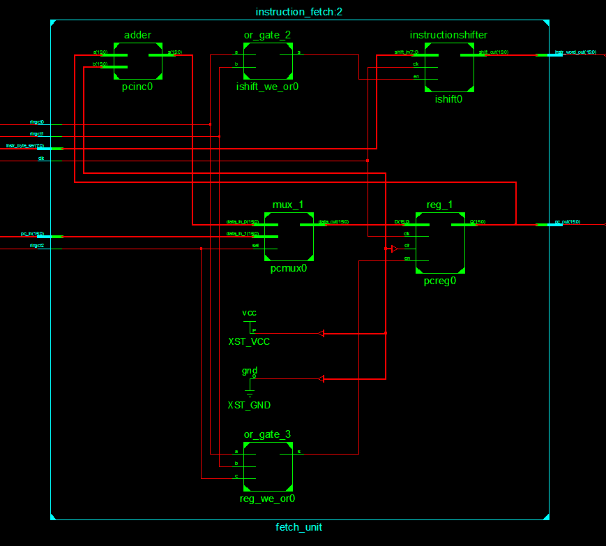
The above code specifies how the aforementioned shift register should be connected to other components in the instruction fetcher. A RTL diagram of the components and their connections:
The code for the shift register is a lot simpler:
library ieee;
use ieee.std_logic_1164.all;
entity instructionshifter is
   port (shift_in  : in  std_logic_vector (7 downto 0);
         clk       : in  std_logic;
         en        : in  std_logic;
         shift_out : out  std_logic_vector (15 downto 0));
end instructionshifter;
architecture behavioral of instructionshifter is
   signal shift_tmp : std_logic_vector (15 downto 0) := (others => '0');
begin
   shift: process(shift_in, clk, en)
   begin
      if (rising_edge(clk)) then
         if (en = '1') then
            shift_tmp <= shift_tmp (7 downto 0) & shift_in;
         end if;
      end if;
   end process;
   shift_out <= shift_tmp;
end behavioral;
The key to the operation of the shift register is in this line:
shift_tmp <= shift_tmp (7 downto 0) & shift_in;
This selects the lower byte of the signal stored in the shift register, concatenates it with the incoming byte, and stores it back in the shift register. Now, on to decoding the instruction.
The first few instructions for the ALU opcode are easy to decode; they share their value with the function bit in the instruction. For the next instructions, the branch instructions, the alu opcode is determined based on the instruction opcode and rt field. Since all of the branches are comparisons to zero, only one operand is supplied, allowing the rt field to be used as a function field.
If this seems strange, this was taken right out of the MIPS Instruction Set; MIPS uses rt as a function register for compare to zero instructions to save opcodes for other instructions that may need more than one register.
In addition to branch instructions, there are load and store instructions that also will require the ALU to calculate the memory address (load immediate does not need addition, but I implemented it anyway for simplicity of designing the execution unit). If the instruction opcode supplied to the decoder is a load or store instruction (3 or 4), then the ALU opcode output should be 2 for addition. This explanation is a bit confusing, but should make more sense with a little bit of code.
alu_tmp <=  "0010" when (is_mem = '1') else
            "1000" when (is_branch = '1' and rt_tmp = "000") else
            "1001" when (is_branch = '1' and rt_tmp = "001") else
            "1010" when (is_branch = '1' and rt_tmp = "010") else
            "1011" when (is_branch = '1' and rt_tmp = "011") else
            "1100" when (is_branch = '1' and rt_tmp = "100") else
            "1101" when (is_branch = '1' and rt_tmp = "101") else
            "0010" when (is_ldi = '1') else
            func (3 downto 0);
The signals is_branch, is_mem, and is_ldi are defined based on the opcode (and for is_ldi, the "rt" field as well).
Now that the instruction decoder can determine the ALU opcode, the operands that the ALU will operate on must also be determined. For the r-type arithmetic instructions, rs and rt are the two registers that contain operands A and B (respectively). rd is the destination register and is not used by the ALU. For both the load and store instructions (and load immediate, again, only for simplicity), the ALU adds operand A with operand B; however, operand B is not from the register file, it is the 8-bit immediate specified by the instruction. This means that a mux must be used to determine whether operand B is an immediate or the contents of rt. The select signal for this mux is actually generated in the execute unit, but uses a 4-bit wide ctl signal generated by the instruction decoder.
The signal for the multiplexer is an or of the following is_ldi, is_store, is_load. Ldi stands for load immediate, and store and load are store and load (duh). These three instructions are the only instructions that use an immediate operand in an arithmetic instruction (branches have a separate adder). The code that generates these three signals is as follows:
with opcode_tmp select
   is_load  <= '1' when "10",
               '0' when others;
with opcode_tmp select
   is_store <= '1' when "11",
               '0' when others;
   is_ldi <= '1' when (opcode_tmp = "01" and rt_tmp = "110") else '0';
   is_branch <= '1' when (opcode_tmp = "01" and (rt_tmp = "001" or rt_tmp = "010" or rt_tmp = "011" or rt_tmp = "100" or rt_tmp = "101")) else '0';