 Nixie
NixieWhen we left, the PMMA trenches where about 200µm wide and 100µm deep. The idea, to further etch it so the bottom of the trench would reveal the substrate below, allowing for, hopefully, 100µm wide stencil bottom.
Soon it was revaled that some spacing (50µm) had to be added in between starts and stops, otherwise, the laser would overetch in the corners because of stepover.
With said spacing, the result was much better:
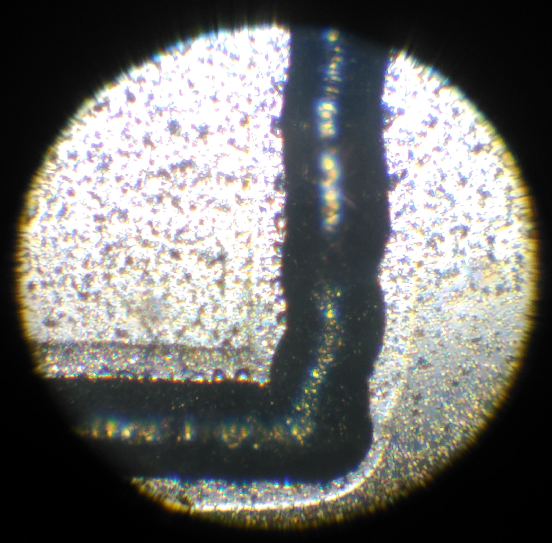
That continued into some paterning* tests:
*(no relation to actual semicon paterning)
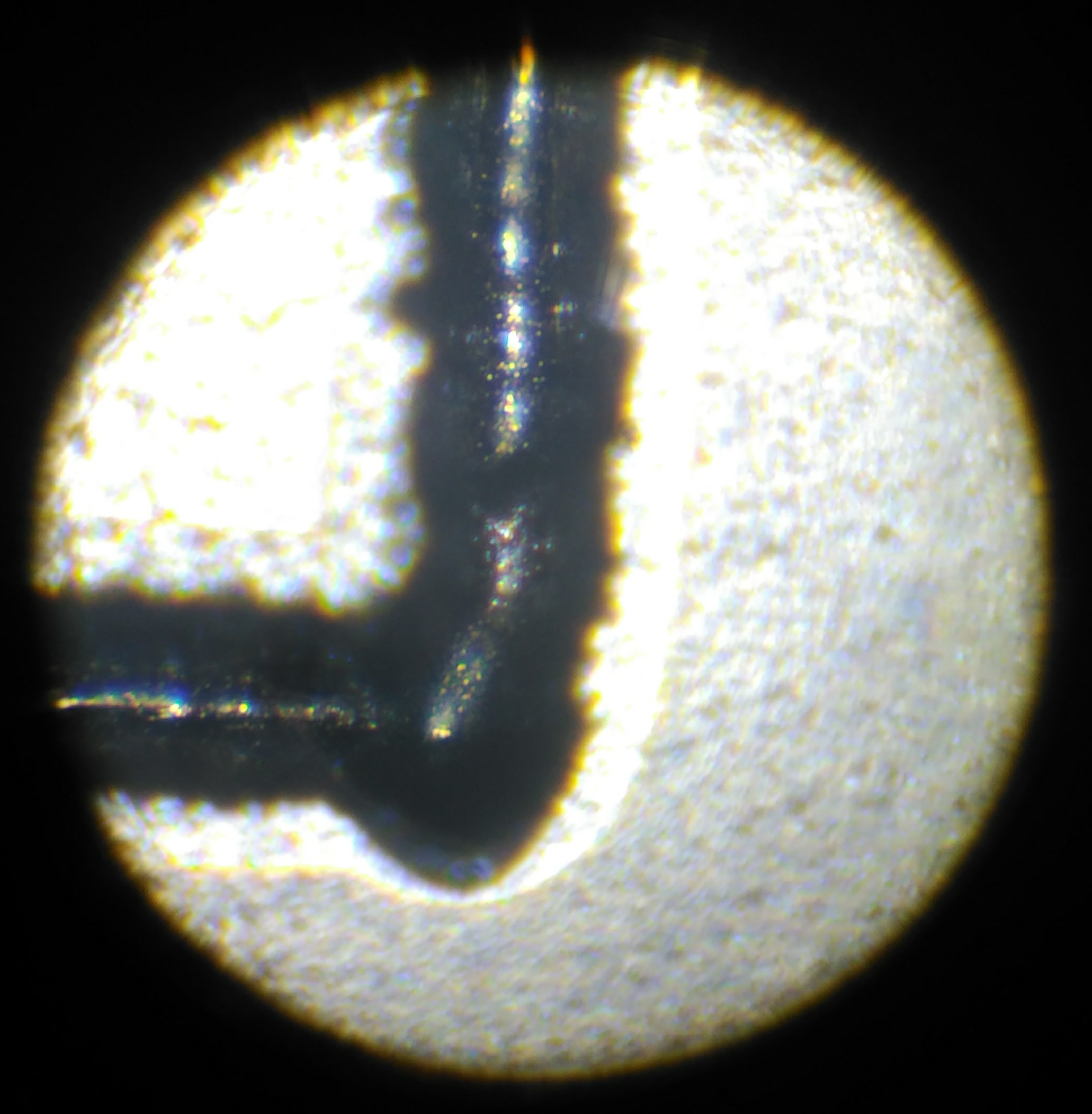
Squareish:
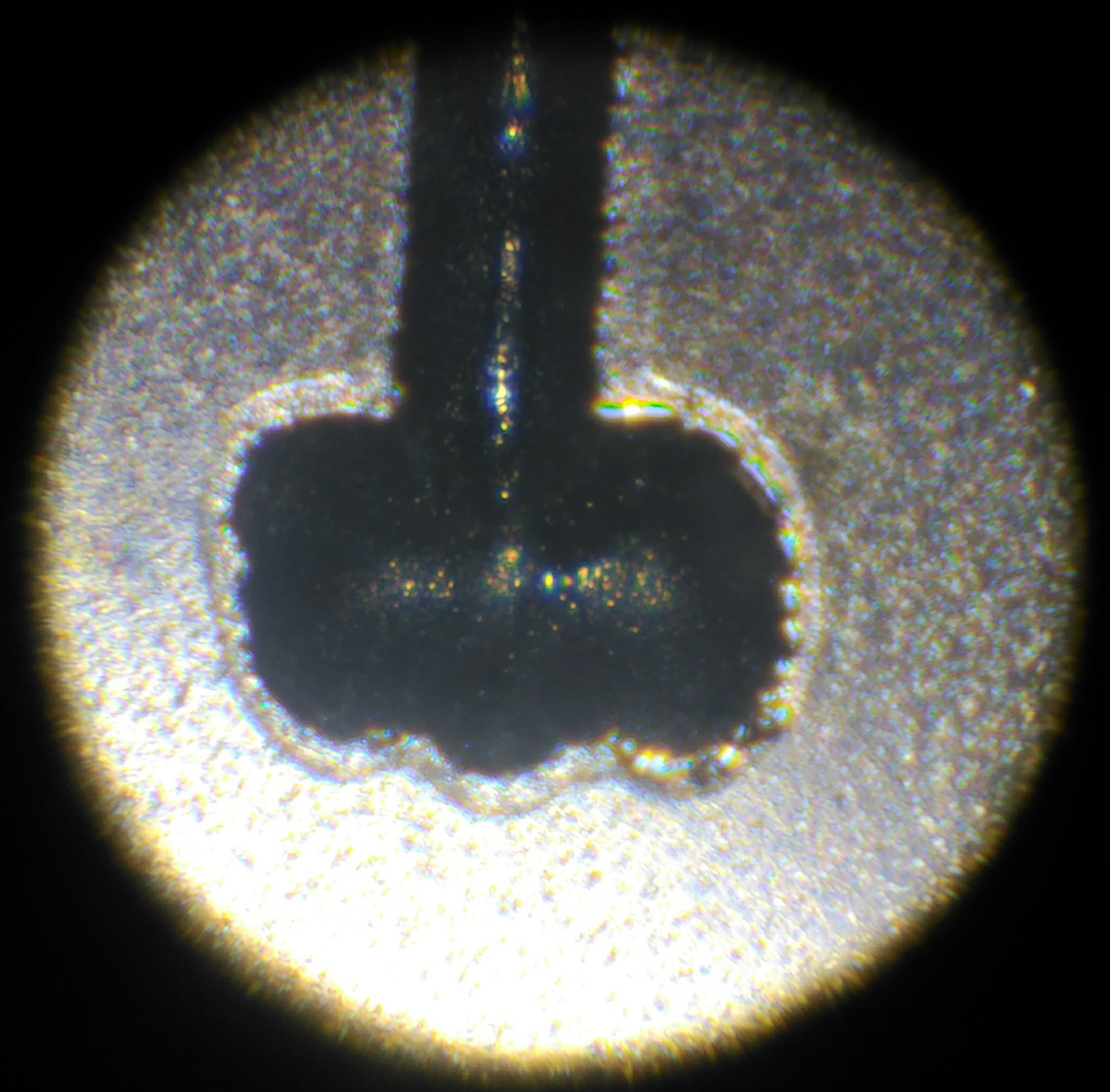
Imaginary fet:
After that, I thought that was it, however, my brain had other plans.
It thought about getting rid of the useless parts of the laser beam, and concentrating on the etching, using a graphite "Hot Trap" as iris. That way, I could increase the power in the laser tube to have more consistency (lowest amperages behave a bit erratically), but not burn through the PMMA layer.
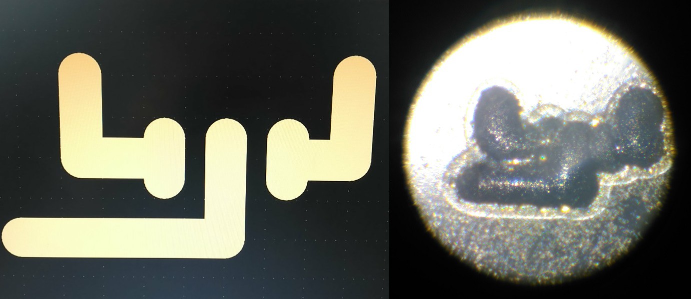
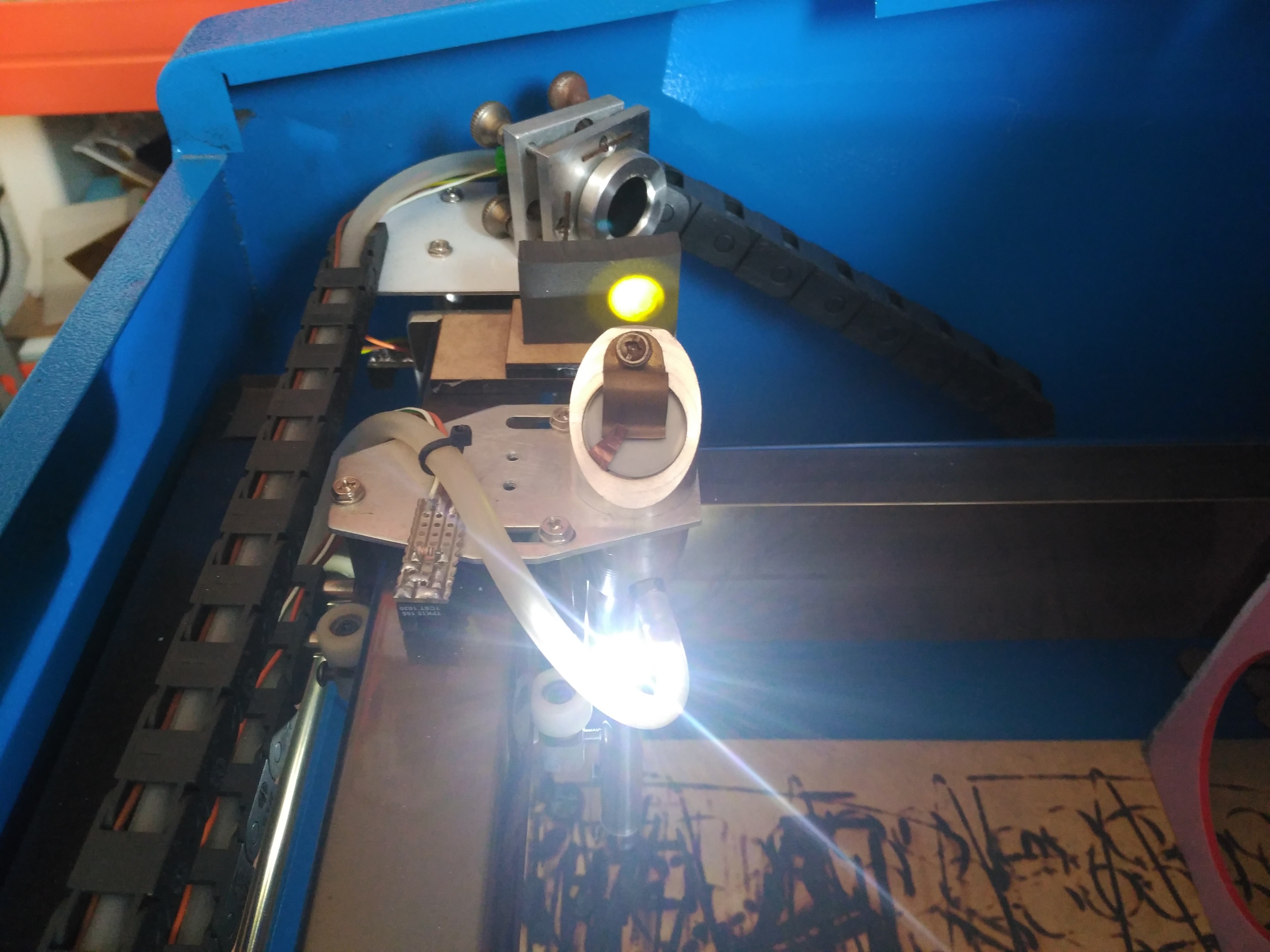 On top: Beam backward tracing with a flashlight so I can position the graphite block.
Result:
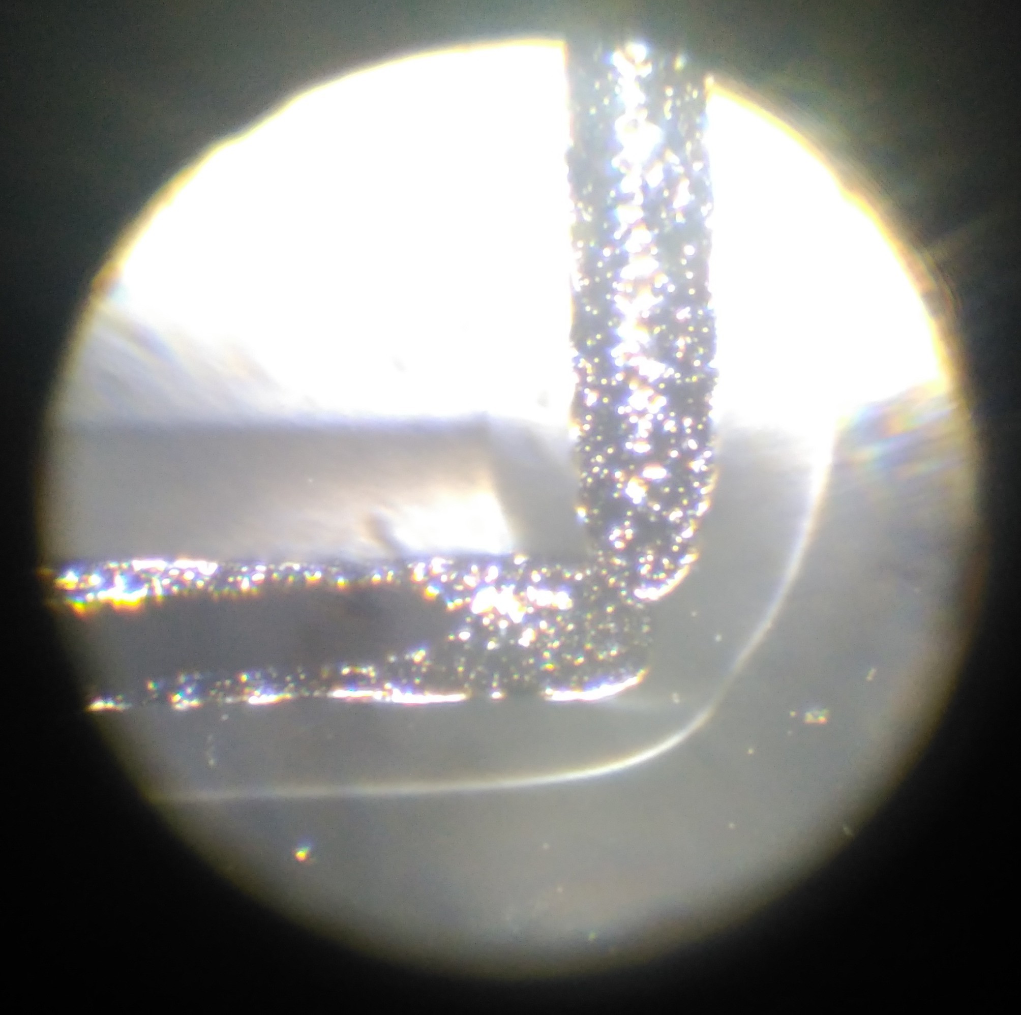
Smaller and much more defined trenches!
About 2/3 the width of previous tests and 50% shallower depth of trench (aout 50µm deep).
Good enough as to have rendered the 50µm spacing obsolete.
This should enable higher precision in the mask, requiring a gap of 25µm between endpoints, and closer spacing between trenches.
I'm having so much fun XDDDD
See you in the next installment!!
Discussions
Become a Hackaday.io Member
Create an account to leave a comment. Already have an account? Log In.