 Nixie
NixieUntil now, I had been doing the laser litography tests with the machine as is. Nailing the focal point was tricky, if I ever found it.
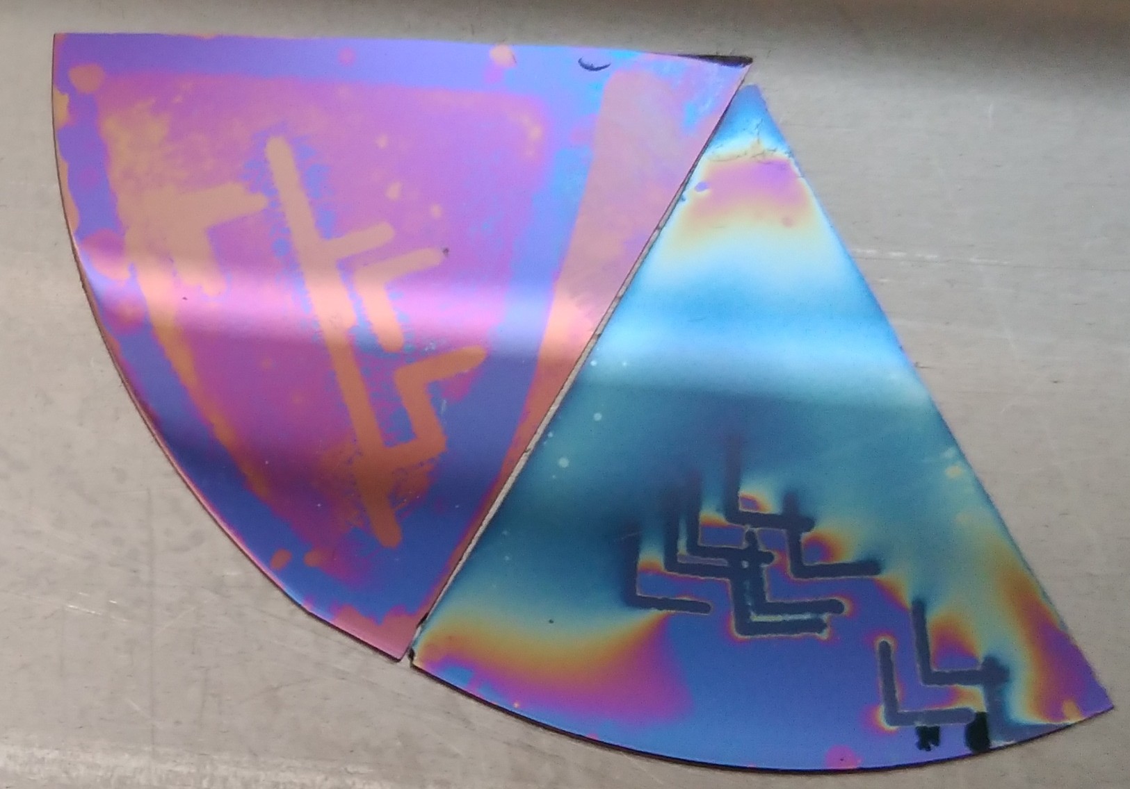
Once I started having better results with the technique (right in the above image) it was clear I needed a better way to find and mantain focus with the silicon.
The holder also has to be hollow, since the laser mostly goes through the Silicon, and having a surface just below the wafer, could prove problematic.
So, holes where drilled...
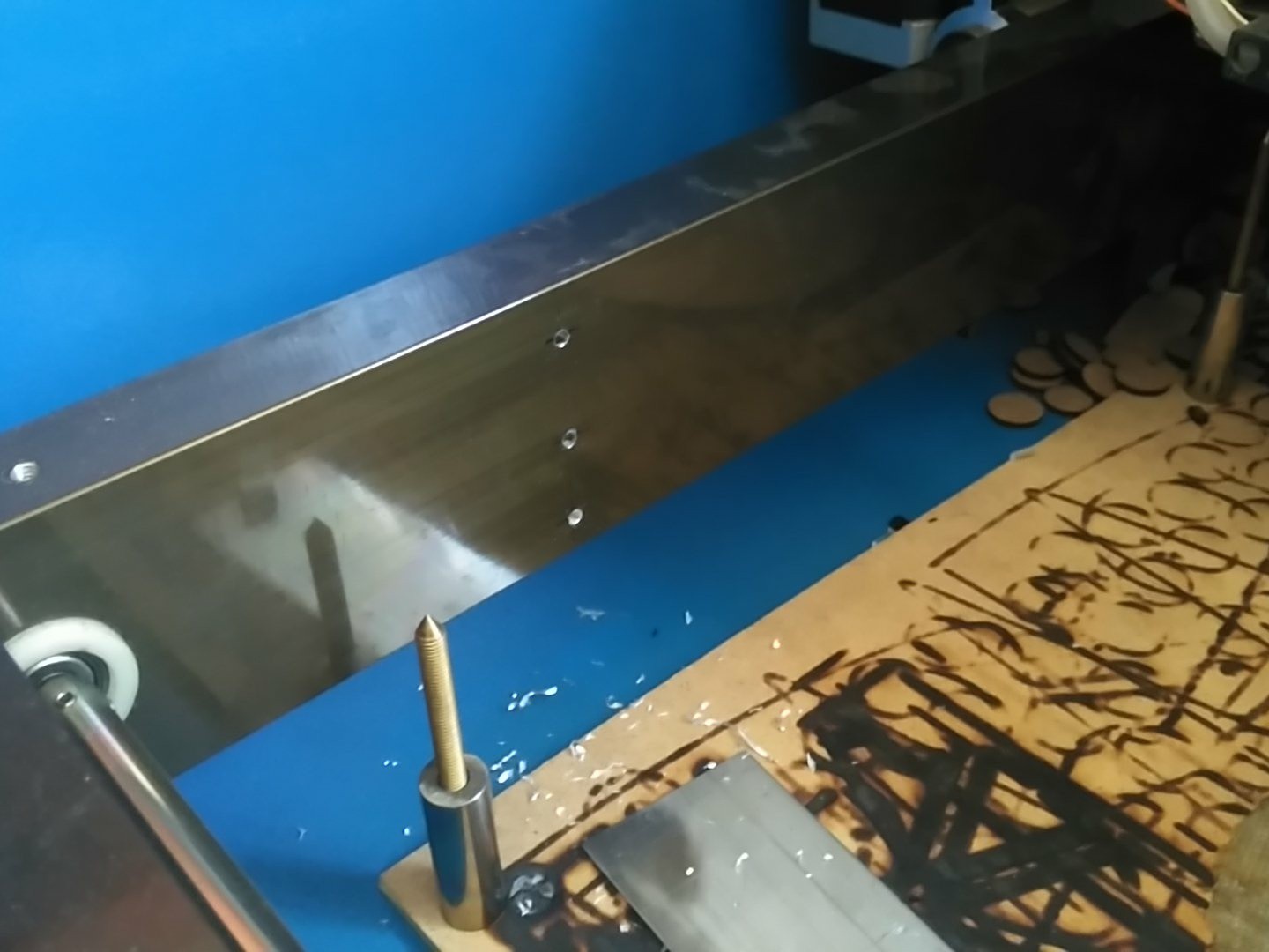
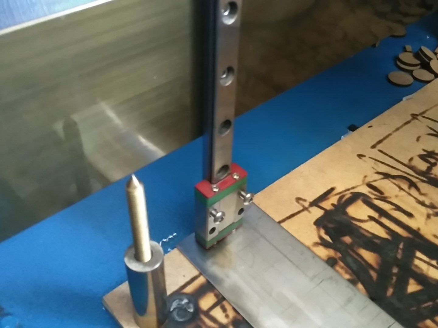
And a vertical linear rail was added:
The design requirements dictated the shape, edges and lengths, so there wasn't much to the design:
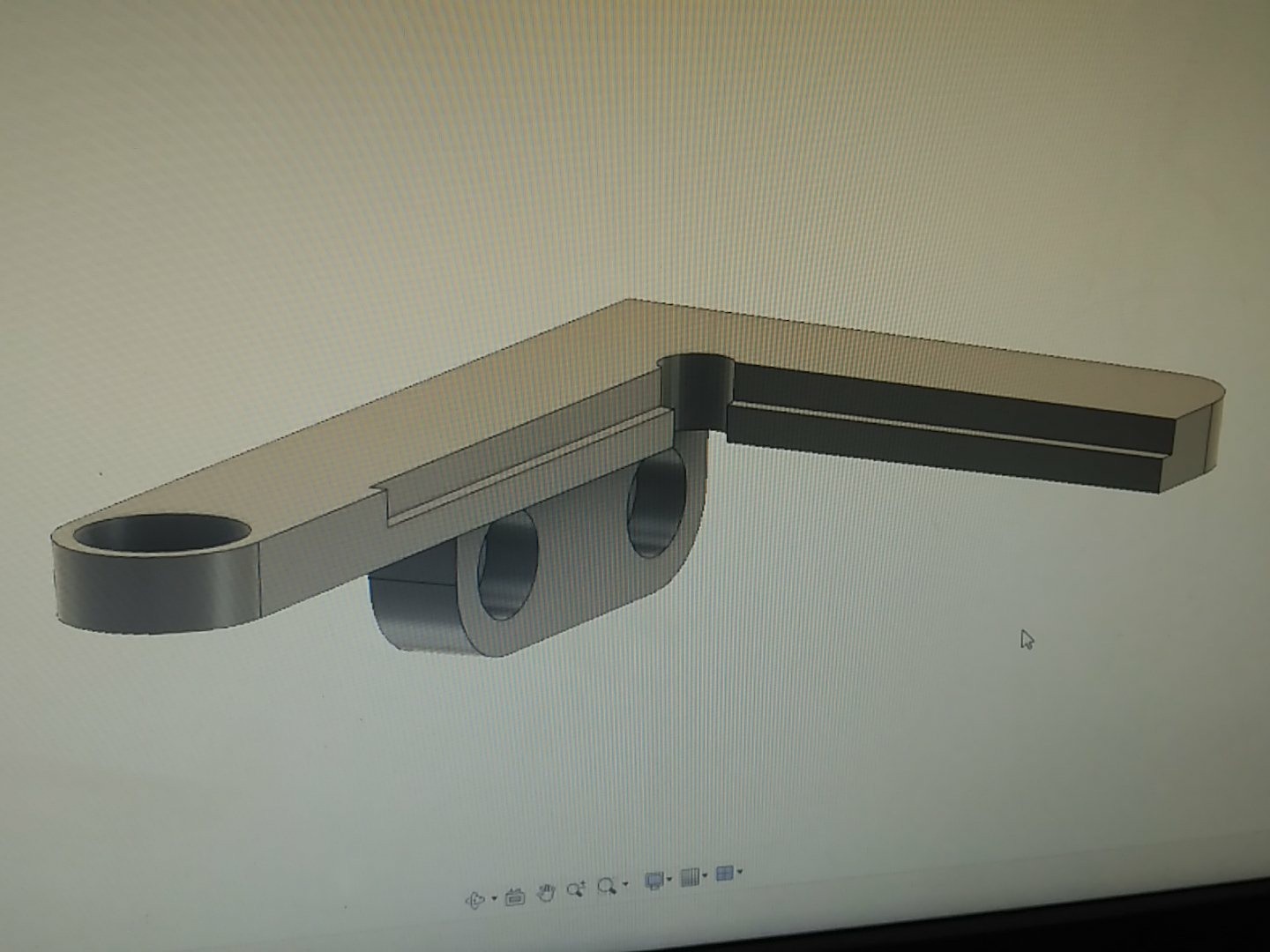
This piece, working near a laser, should not be made out of plastic, however, for quick tests, I 3D printed it to have a feel of how it sat in the machine.
(Just ignore the bearing, it was meant for something else, but it was not needed in the end.)
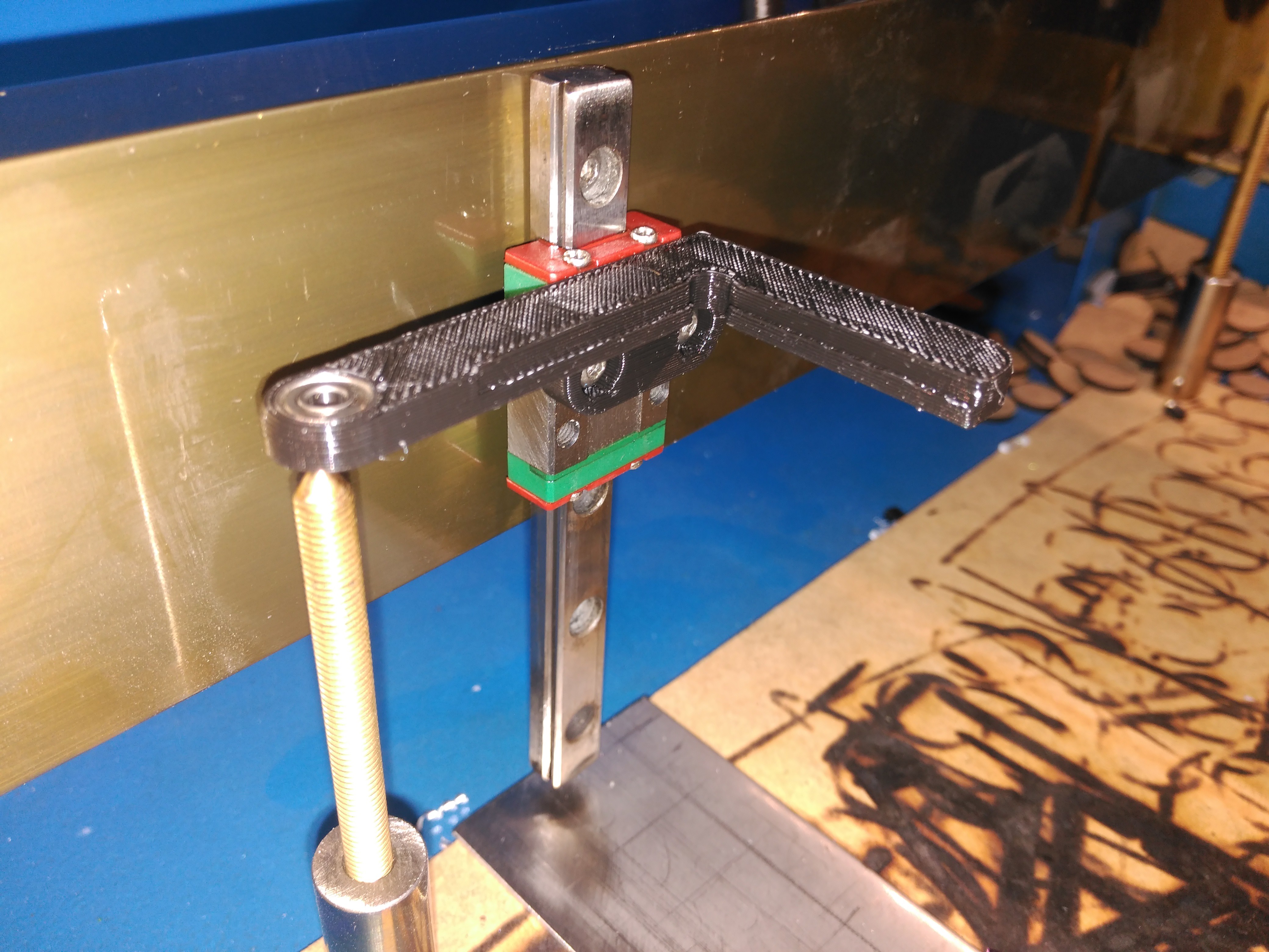
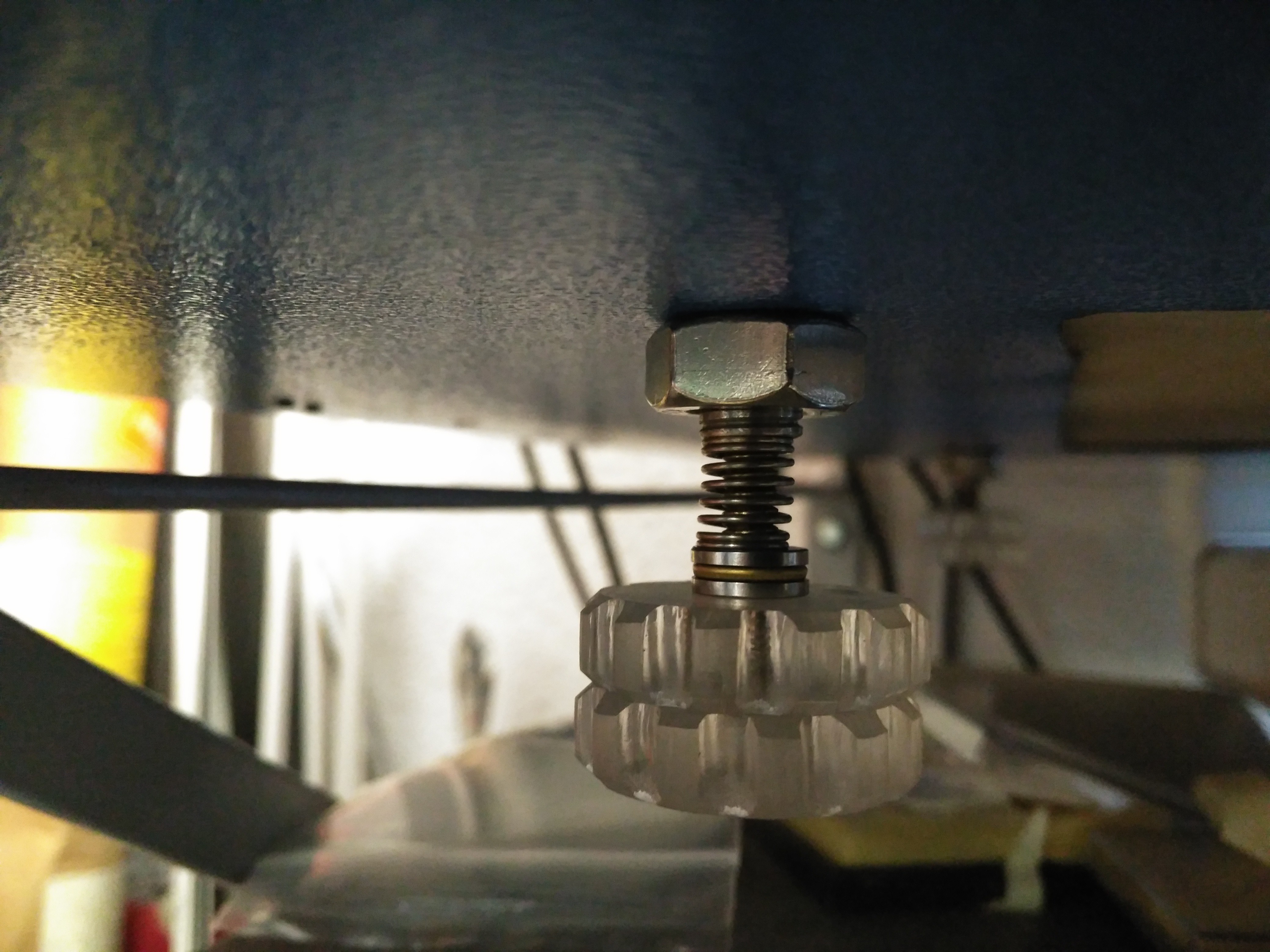
I will be using the cutting height adjusters, however, just as they where, it could probe flimsy for precision height adjustment, so the screw was preloaded with a spring and an axial bearing to prevent twist resistance:
Everything looked great, so I embarked in the machning. Nothing in it was size critical, only the mounting holes, so I preferred to hand machine it, as my mill can remove much more material than my cheap CNC router can.
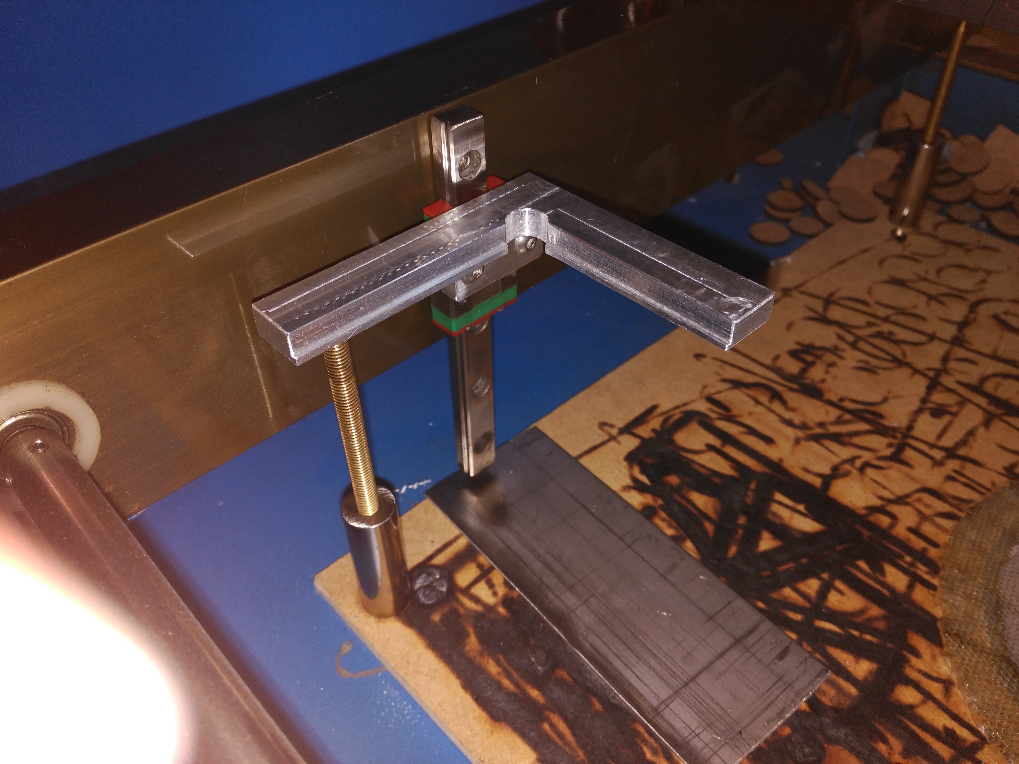
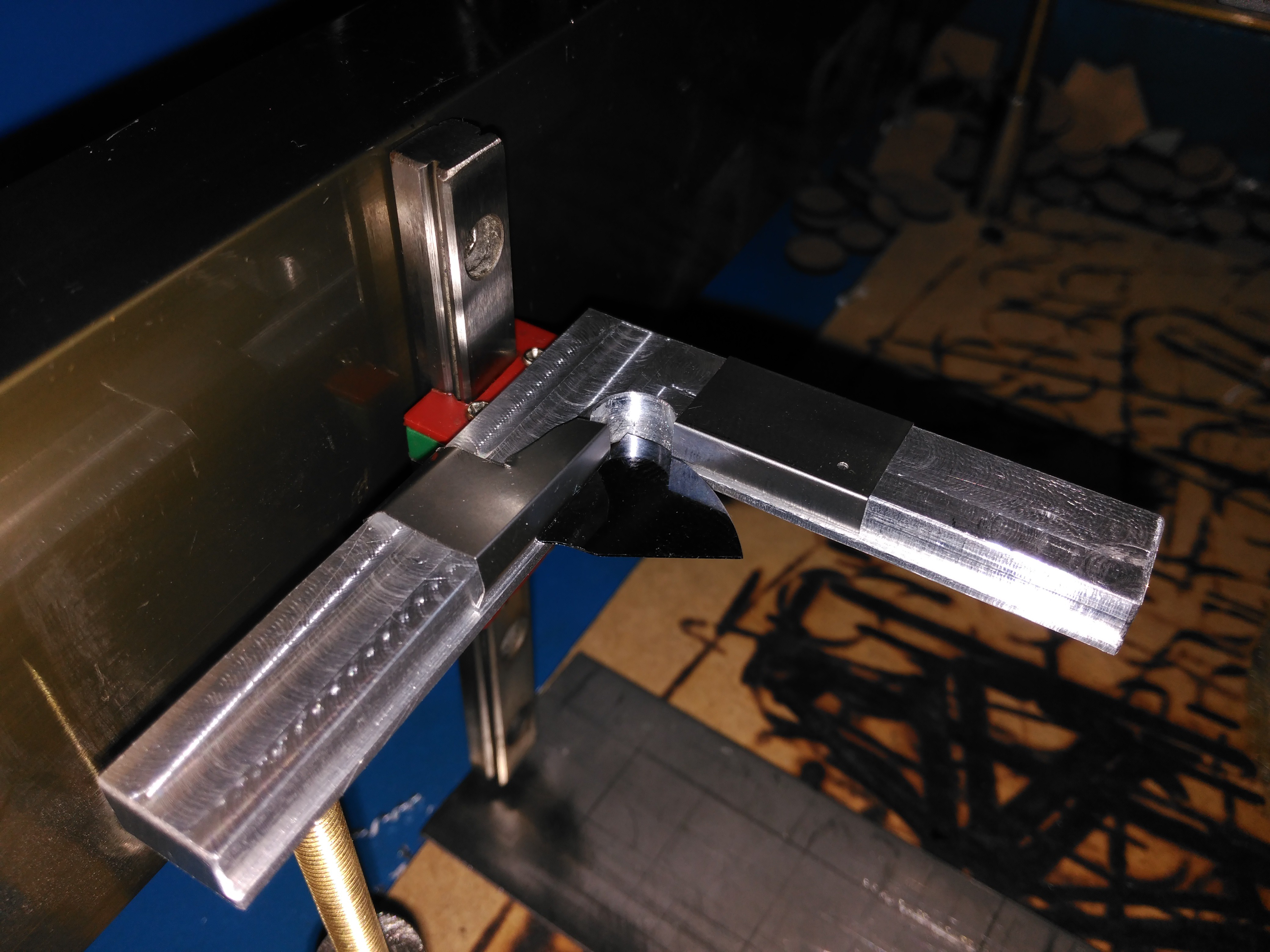
Holding is done through flat springs, sitting against the small 1mm ledges in the piece, and made pretty much like the cover in the hot plate:
(The ones in the image are just temporary, better ones will be made. To prevent chipping, the side in contact with the silicon is rolled, so it presents a smooth surface.)
Done!
Now, let's keep R+D going!
Discussions
Become a Hackaday.io Member
Create an account to leave a comment. Already have an account? Log In.