 Ever
EverThen the design of electrical hardware version 1.0 of the project is presented. Any suggestions or implement necessary changes be annexed to this version.
Milestones to achieve in the project are:
- Increase MFC voltage rating with 2 or more cells. Today it has a voltage of 0.3 V
- Define the current range for output device (Ioad). For version 1.0 is has Vout = 0 to 4 mA
- Improve design robustness to ensure external conditions do not cause any failures.
- Optimal values for Cstore and Cout.
- Ability to control one load (switch on/off of a LED) – either to allow for greater capacity, or timing control of when the output is on or off.
Design approach:
It is in the initial stage of the project. The defined electrical hardware architecture consists of a set-up converter with the LTC3108. The design schematic diagram was made with the DesignSpark PCB program which has free license. For now the library has been built LTC3108 component with its respective footprint and encapsulation type is DFN. It proceeds to place the libraries available in DesignSpark PCB. Efficiency is key in the design, but through this device do not have optimal efficiency percentage. The primary objective is to demonstrate the power of an LED of the collected energy of a plant. Later it will be necessary to create a version 1.1 that allows to increase the current capacity in order to feed various types of electric charges.
A modular design should also make the development process a bit easier, since we can do testing onthemodules without having to test the complete capacity.
Design stages
The first steps of the design are to look at the following:
- Define of the ratio of voltage and current.
- Selection of the components. Transformer ratio, Cstore and Cout sizing.
- inductor sizing, design and its impact on efficiency
- Test of the MFC operation for energing harvesting.
Using a small step-up transformer, the LTC3108 provides a complete power management solution for power different types of load. A storage capacitor provides power when the input voltage source is unavailable. Extremely low quiescent current and high efficiency design ensure the fastest possible charge times of the output reservoir capacitor.
COMPONENT SELECTION
Step-Up Transformer
The step-up transformer turns ratio will determine how low the input voltage can be for the converter to start. Using a 1:100 ratio can yield start-up voltages as low as 20mV. Other factors that affect performance are the DC resistance of the transformer windings and the inductance of the windings. Higher DC resistance will result in lower efficiency. The secondary winding inductance will determine the resonant frequency of the oscillator, according to the following formula.
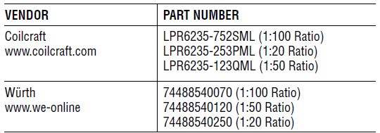
Table 1. Recommendation of the manufacturer for choice of the transformer.
C1 Capacitor
The charge pump capacitor that is connected from the transformer’s secondary winding to the C1 pin has an effect on converter input resistance and maximum output current capability. Generally, a minimum value of 1nF is recommended when operating from very low input voltages using a transformer with a ratio of 1:100. Too large a capacitor value can compromise performance when operating at low input voltage or with high resistance sources. For higher input voltages and lower turns ratios, the value of the C1 capacitor can be increased for higher output current capability. Refer to the Typical Applications schematic examples for the recommended value for a given turns ratio.
VOUT and VSTORE Capacitor
For pulsed load applications, the VOUT capacitor should be sized to provide the necessary current when the load is pulsed on. The capacitor value required will be dictated by the load current, the duration of the load pulse, and the amount of voltage droop the circuit can tolerate. The capacitor must be rated for whatever voltage has been selected for VOUT by VS1 and VS2.
The VSTORE capacitor may be of very large value (thousands of microfarads or even Farads), to provide holdup at times when the input power may be lost. Note that this capacitor can charge all the way to 5.25V (regardless of the settings for VOUT), so ensure that the holdup capacitor has a working voltage rating of at least 5.5V at the temperature for which it will be used. The VSTORE capacitor can be sized using the following:
Where 6μA is the quiescent current of the LTC3108, IQ is the load on VOUT in between bursts, ILDO is the load on the LDO between bursts, IBURST is the total load during the burst, t is the duration of the burst, f is the frequency of the bursts, TSTORE is the storage time required and VOUT is the output voltage required. Note that for a programmed output voltage of 5V, the VSTORE capacitor cannot provide any beneficial storage time.
To minimize losses and capacitor charge time, all capacitors used for VOUT and VSTORE should be low leakage. See Table 2 for recommended storage capacitors.
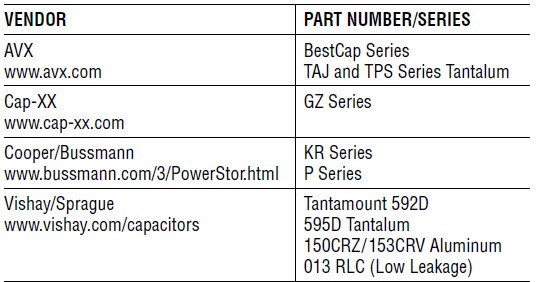
Table 2. Recommendation of the manufacturer for choice of the supercapacitor.
Storage capacitors requiring voltage balancing are not recommended due to the current draw of the balancing resistors.
Charge Pump and Rectifier
The AC voltage produced on the secondary winding of the transformer is boosted and rectified using an external charge pump capacitor (from the secondary winding to pin C1) and the rectifiers internal to the LTC3108. The rectifier circuit feeds current into the VAUX pin, providing charge to the external VAUX capacitor and the other outputs.
The PGD signal can be used to enable a sleeping microprocessor or other circuitry when VOUT reaches regulation, indicating that enough energy is available for a burst.
Discussions
Become a Hackaday.io Member
Create an account to leave a comment. Already have an account? Log In.