 Yann Guidon / YGDES
2016-10: this project is now shelved. The probe point of my Tektro scopes have insuficient amplitude...
This project is more about designing an energy-harvesting device that can accomodate various oscilloscopes, rather than design the best differential probe circuit. I am not skilled enough to develop such delicate and precise analog circuitry but I am able to design a step-up power supply. I hope to learn more about oscilloscope black magic as well ;-)
Logs:
1. BNC trick
2. Hoarders' delight
3. System analysis and design
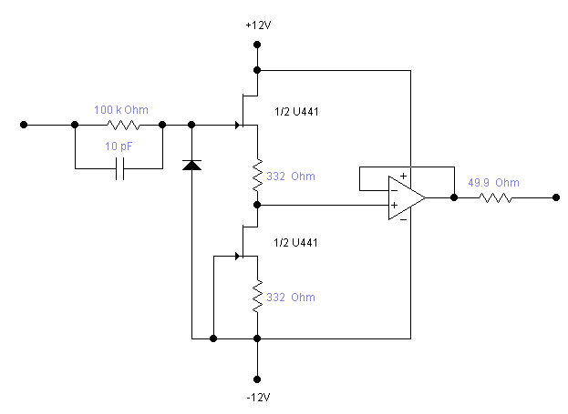
4. Amplifier design
5. BNC mess
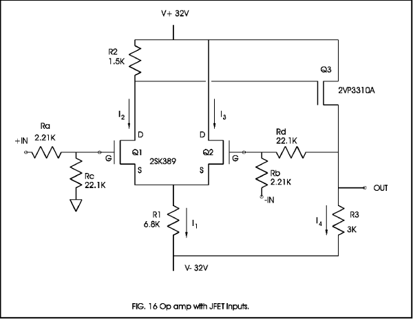
6. Input FET stage
 (No, I'm not shooting for GHz precision, my fastest scope reaches 200MHz only)


 Szoftveres
 Pero
Pero
 Paul Andrews
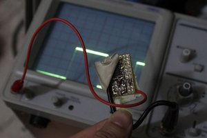
More links to (active and passive) probe designs (from https://hackaday.io/page/2628-needing-p6243-or-similar-1ghz-active-probes/discussion-72392) :
http://paulorenato.com/index.php/93
http://www.eevblog.com/forum/projects/good-design-for-a-diy-active-probe/
https://easyeda.com/andyfierman/project-g2QNnljhf
https://easyeda.com/guest/High_impedance_probe_using_opamp-gmtnFzRL3
http://www.sigcon.com/Pubs/straight/probes.htm
(thanks Ted)