 Kuldeep Singh Dhaka
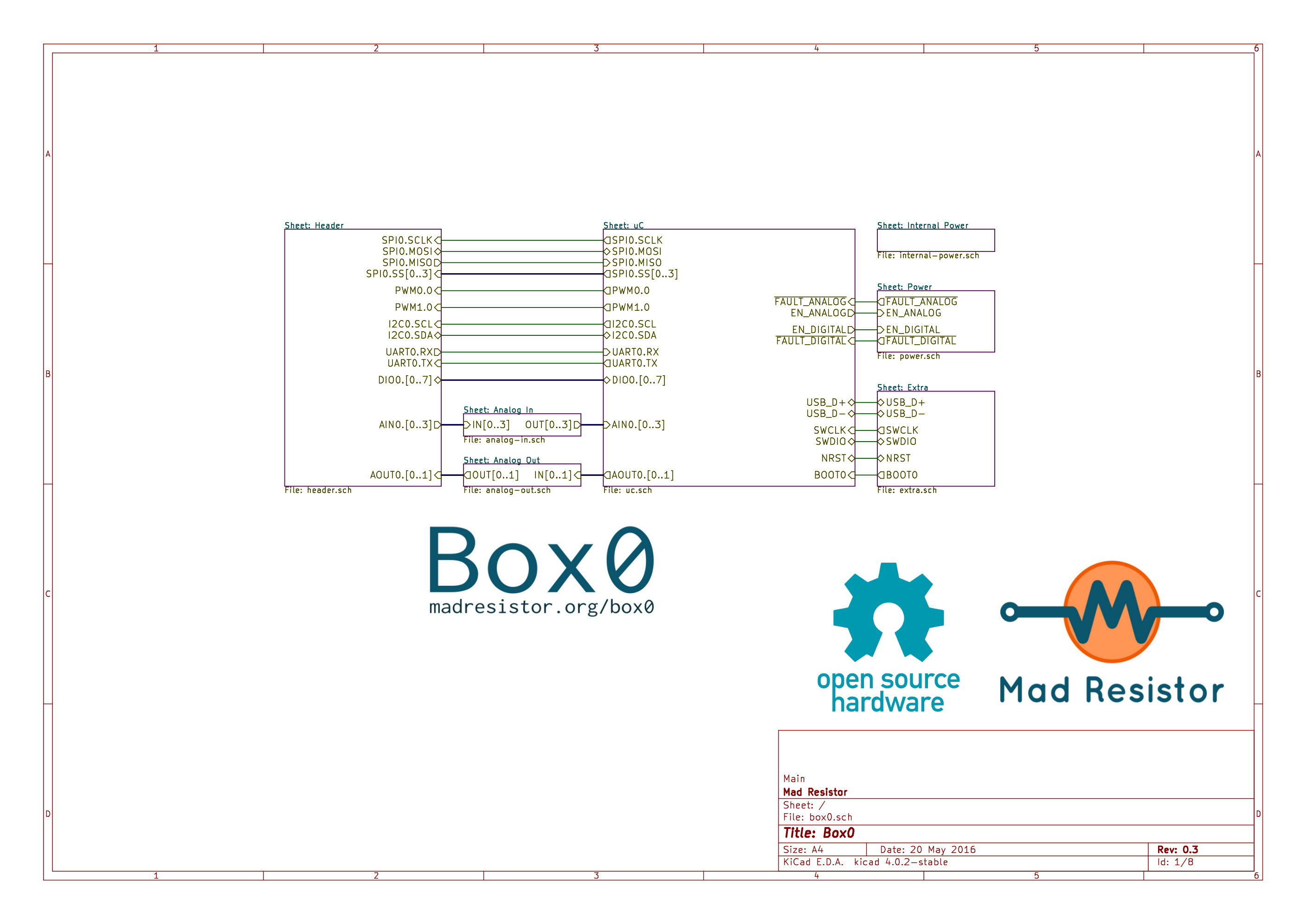 Click on image for higher resolution.
(For complete schematic in PDF click here)
The first sheet contains a high level overview of the schematics.
The design has been divided into different subsystems which interact with each other in an abstract manner.The schematic for these subsystems has been put in their respective sheets.This helps to reduce the clutter, provides better design management, ease of readability and usability.
We will explain a bit about different subsystems one by one to help you get an idea.
Sheet: uC
This block mainly does the following
- Communication (USB, SPI, I2C...)
- Control and coordination of power management ICs
- ADC input and DAC output.
- Digital input and output
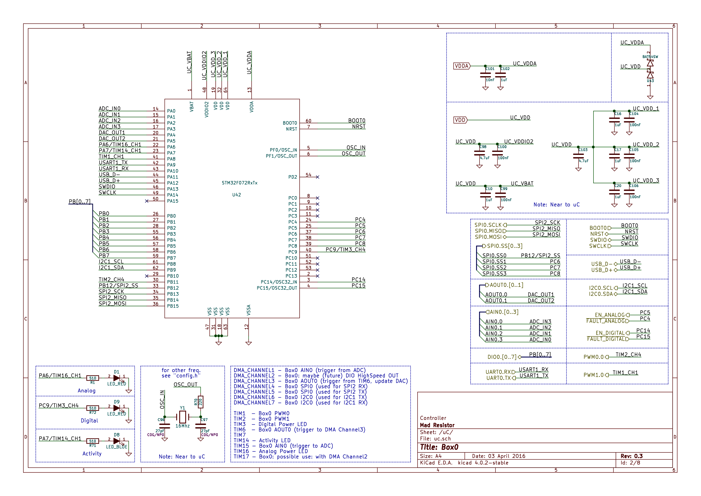
Top Left: The microcontroller STM32F072 - ARM Cortex M0.
- USB FS (12Mbit)
- ADC 1MSPS, 12 bit
- DAC 1MSPS, 12 bit
- DMA 7 channel
- I2C upto 400Khz
- SPI upto 36MHz
- CAN
- Alot more, see full specification.
Top Right: Proper power supply decoupling and bypassing capacitors for analog and digital parts of microcontroller as per recommendations in datasheet.
Top Right extreme corner: if you noticed there is a schottky diode BAT54SW connected between VDDA and VDD of the uC to make sure the potential difference between both the pins remains within safe limit (mainly during startup when power supplies are from different sources, fro e.g when the optional voltage reference for VDDA is used on Box0)
Bottom Left: These are led for activity, power, power-fault indication.
Middle Right: Various pins of microcontroller connected/named/converted according to Box0 pins specification.
Bottom Middle: The list of DMA channel, Timers used for
which task and which peripherial pins are being used for what purpose.
At bottom and right to the led is the crystal oscillator for a clean and stable (10-30 PPM)clock signal to the microcontroller.This works well for our requirements.Though the microcontroller has a RC oscillator built-in but it is no match for a good crystal.
Sheet: Internal power
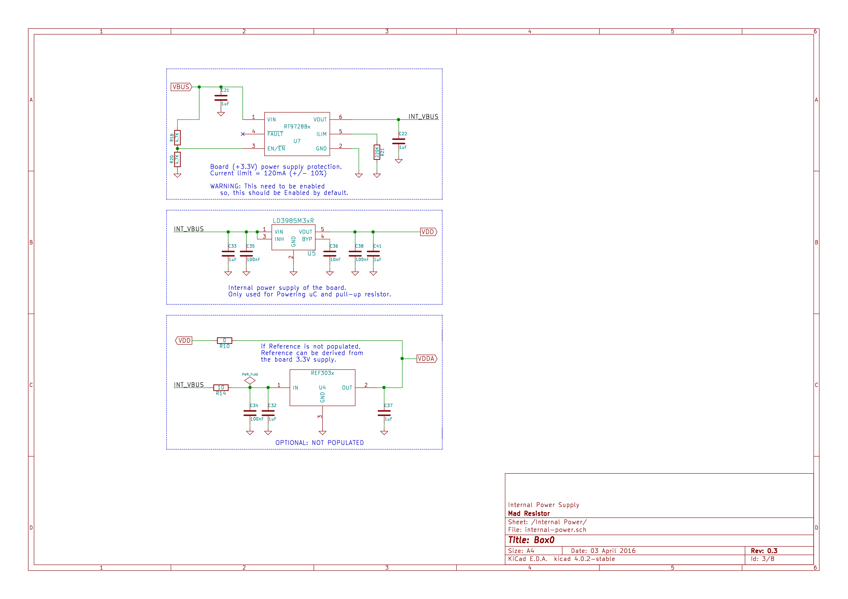
Box0 consist dedicated power supplies for internal and external use.
The internal power supply sheet consist of power managements parts to power the board components only (includes microcontroller).
The power supply automatically turns itself off in case of short circuit or if the current limit exceeds above a certain programmed level.
Top box: RT9728 for active current limit on power coming from USB (in case something bad goes on the board).
Middle box: a 3.3V regulator
Bottom box: a 3.3V [optional] precision reference.
If the precision reference is not populated, it can be connected to the above 3.3V voltage regulator.
The (virtual) power output from this sheet is not provided to user (ie external use).
(except - precision reference which can be used for external use too via "VREF" pin which at the output of which a resistance is placed to limit the currents to safe level during accidental shorts circuits by the user)
Sheet: Extra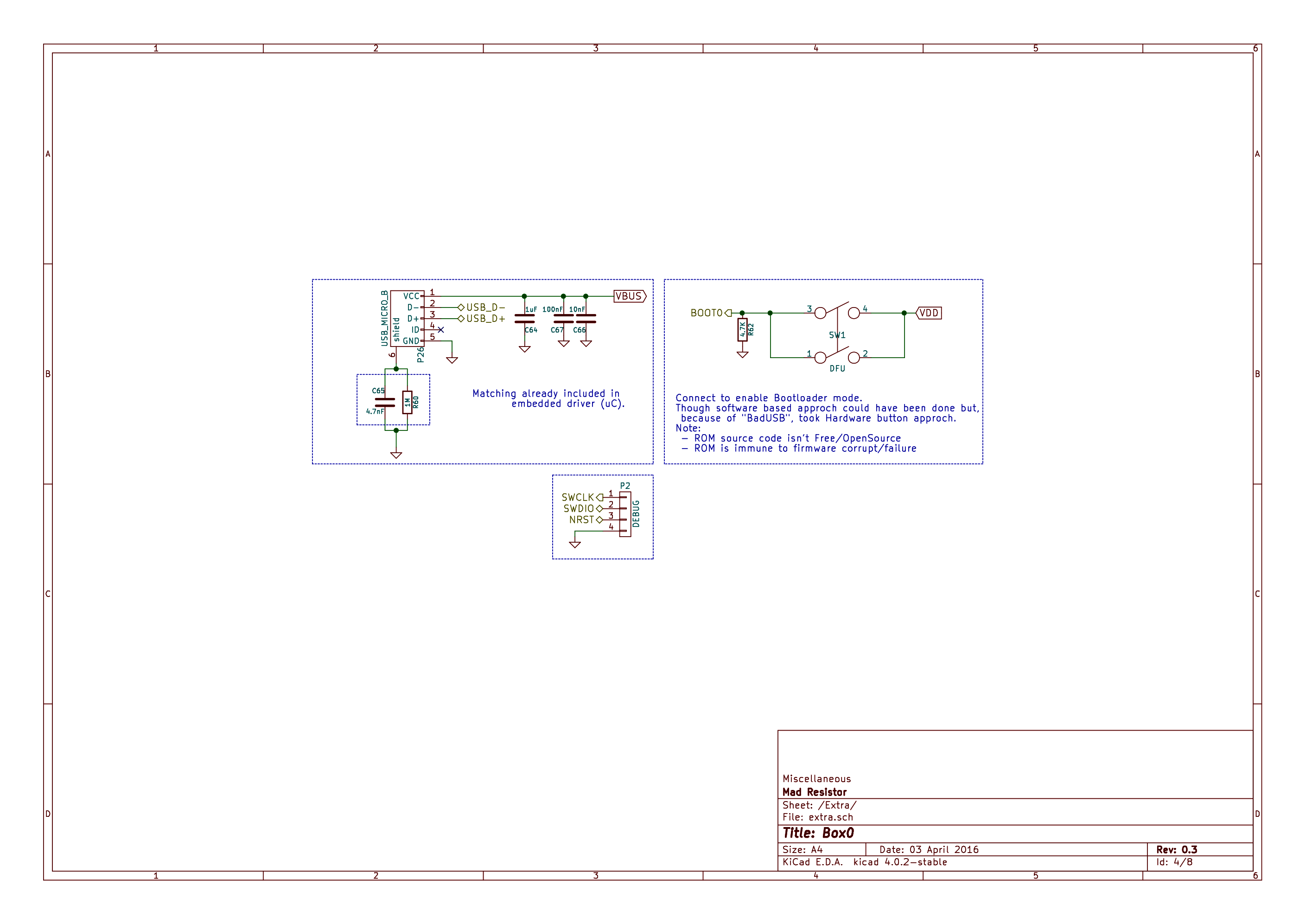
The USB connector, debug pin (SWD) and the BOOT0 (for DFU) button.
Special story for BOOT0 button:
If you are familiar with BadUSB which has also been documented by hackaday here (which @Kuldeep Singh Dhaka tipped off ;).
In order to prevent BadUSB, the BOOT0 button is placed.
When user press the button, the device boot from ROM (proprietary* code by ST).
When it boot from ROM it comes up as a DFU device (USB DFU class - Device Firmware Update).
Only the firmware can be updated when the user want to. There is no possibility of automatic firmware update which do not fullfill the BadUSB requirement.
and btw, if someone can flash malice code to your device, they can do more nasty things.
* = though the ROM is proprietary, just trade-off.
In future we can implement the functionality via flash code.
Also, we can even start a full-fledged project that allow [same flashing api, multiple vendor support] for ARM microcontroller - something like UBOOT for microcontroller ;).
future is bright, lets see!
Sheet: Power
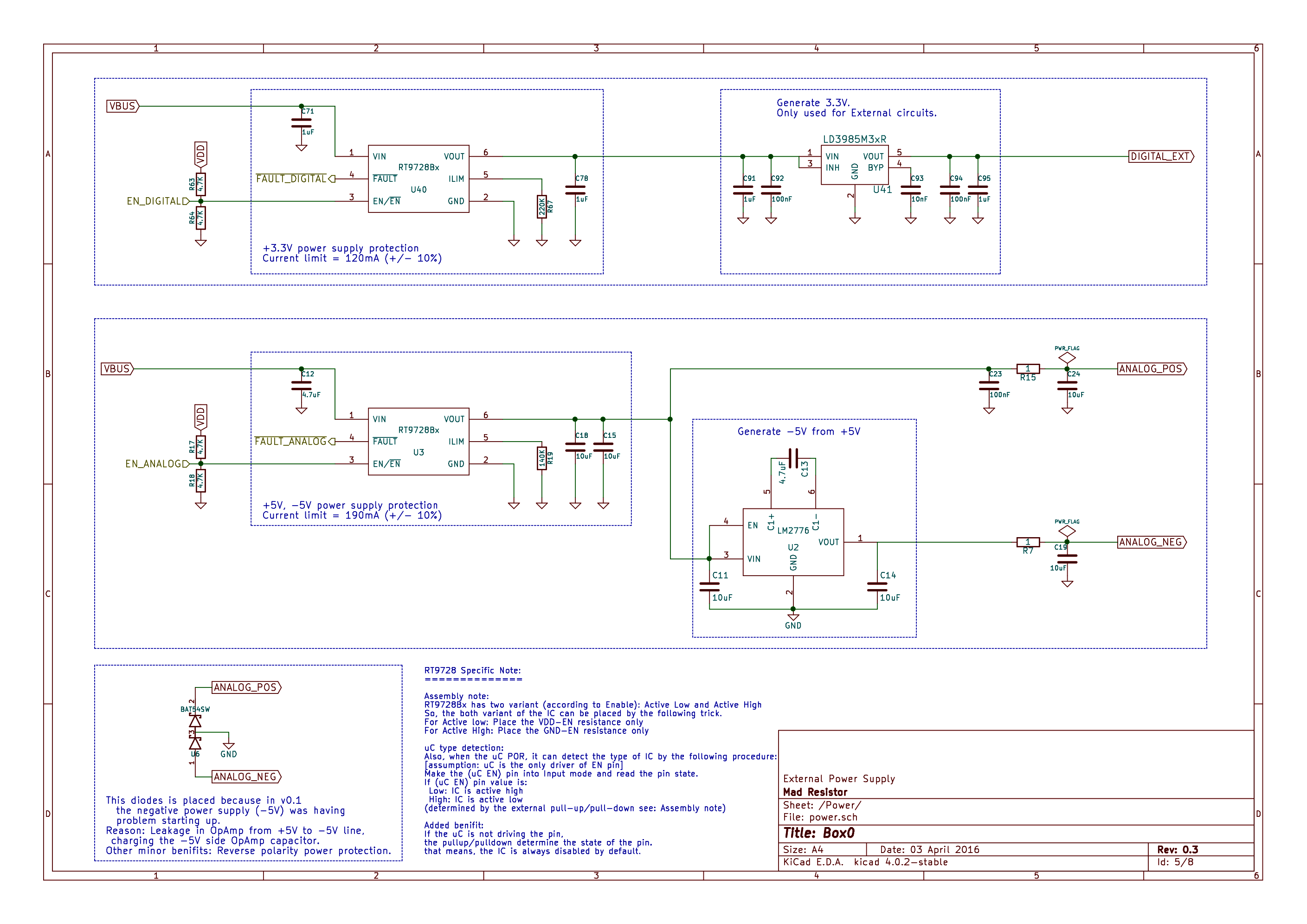
Having onboard short circuit protected and commonly used 3.3V , +5V, -5V is a very helpful for the user while prototyping different type of analog and digital circuits.The power supplies are also quite usable in terms of noise level and current output.
- +5V - active current limit
- -5V - active current limit
- +3.3V - active current limit
In case, the RT9728 current* exceed an interrupt is generated for microcontroller.
* = current limit is set by resistance
Note: The +5V and -5V is also used for powering on board OpAmp's. trade-off because placing another +5V, -5V circuit was costly.Practically its a good tradeoff and we never faced any issues in usability.
Sheet: Analog In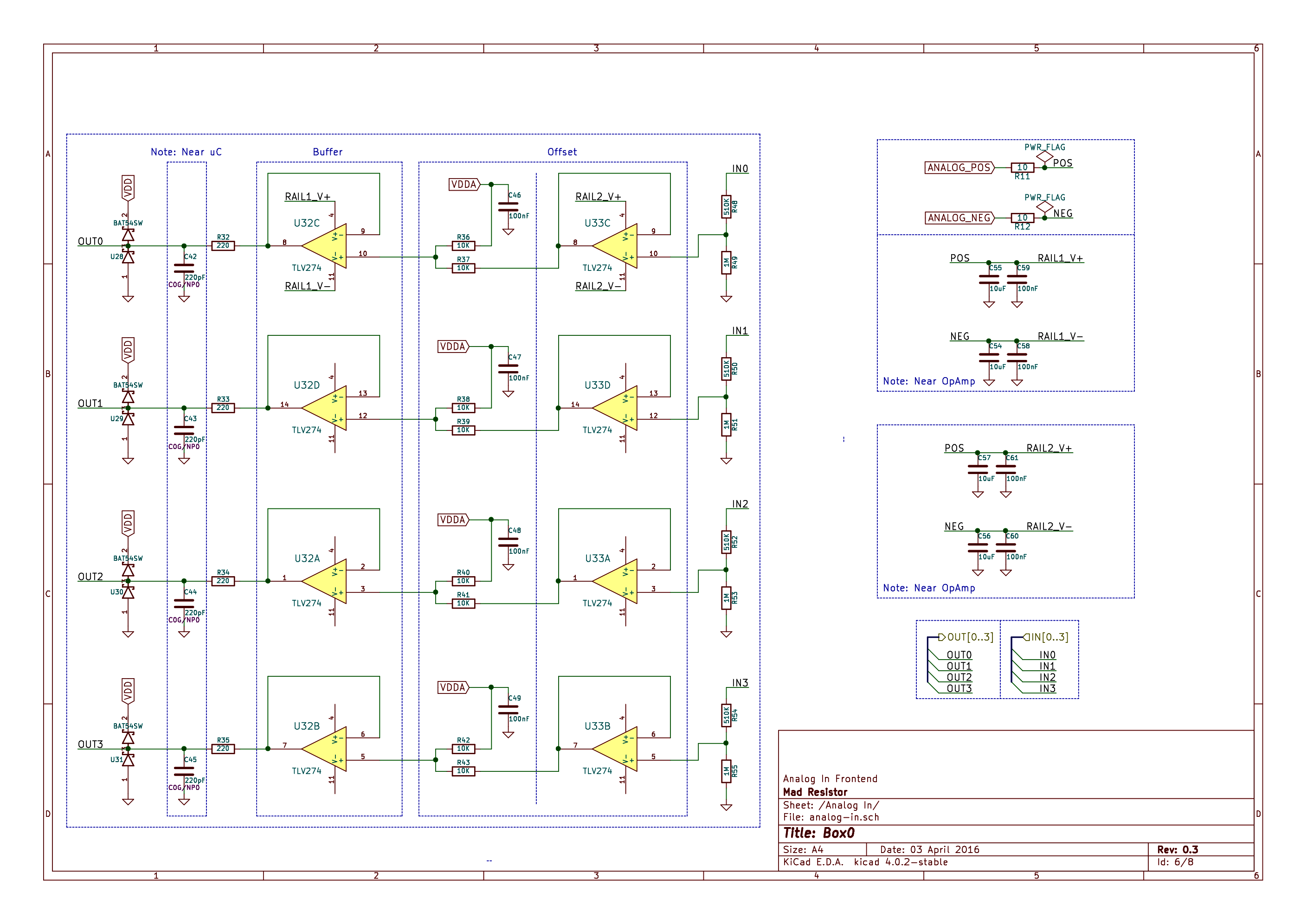 Aim: Condition the external bipolar signal (input range depend upon the ratio of voltage divider) signal to fit the acceptable level of 0V to +3.3V of the internal SAR ADC or micro controller.
Basically: Input-> divide -> buffer -> offset -> buffer->filter->over voltage protect-> feed to ADC input.
We are using TL274 Opamps from Texas instruments.
These have very high input impedance and almost negligible input bias current and has rail to rail o/p capability along with low power consumption.The bandwidth and slew rate suffice for our purpose for feeding the SAR ADC sampling rate.
Also, if you noticed, there four capacitors used in the RC filter which is connected to the opamp output just before the ADC inputs.
These are Class I dielectric "C0G/NP0" capacitors which do not distort the signal quality as compared to other dielectrics such as X7R or X5R whose capacitance varies with applied voltage.
These capacitors work to filter the input signal to the SAR ADC and also work as charge storage for proper sampling of the SAR ADC thus isolating the the opamp output from the transient caused by the input sampling circuit phenomenon.Also these capacitors absorbs the charge
capacitor on each OpAmp output pin. Specially designated with "C0G/NP0". These are 1st class dilectric special capacitors and offers very low distortion as compared to other ceramic capacitors.
Everyone learned from physics text books that capacitance depends on geometry.
Engineering side: capacitance can depend on other factors too : temperature, boasing voltage.
Generally available capacitors have different capacitance at different voltages. (ie capacitance is a function of voltage too).
So, when a heigher voltage signal comes in, capacitance varies, and charging behaviour changes, so the signal is also affected - final: distorts the signals.
Similar type of "COG/NP0" capacitors are also used for crystals (see: microcontroller subsheet) in this case primarily because these capacitors are quite stable with temperature and has good long term stability.
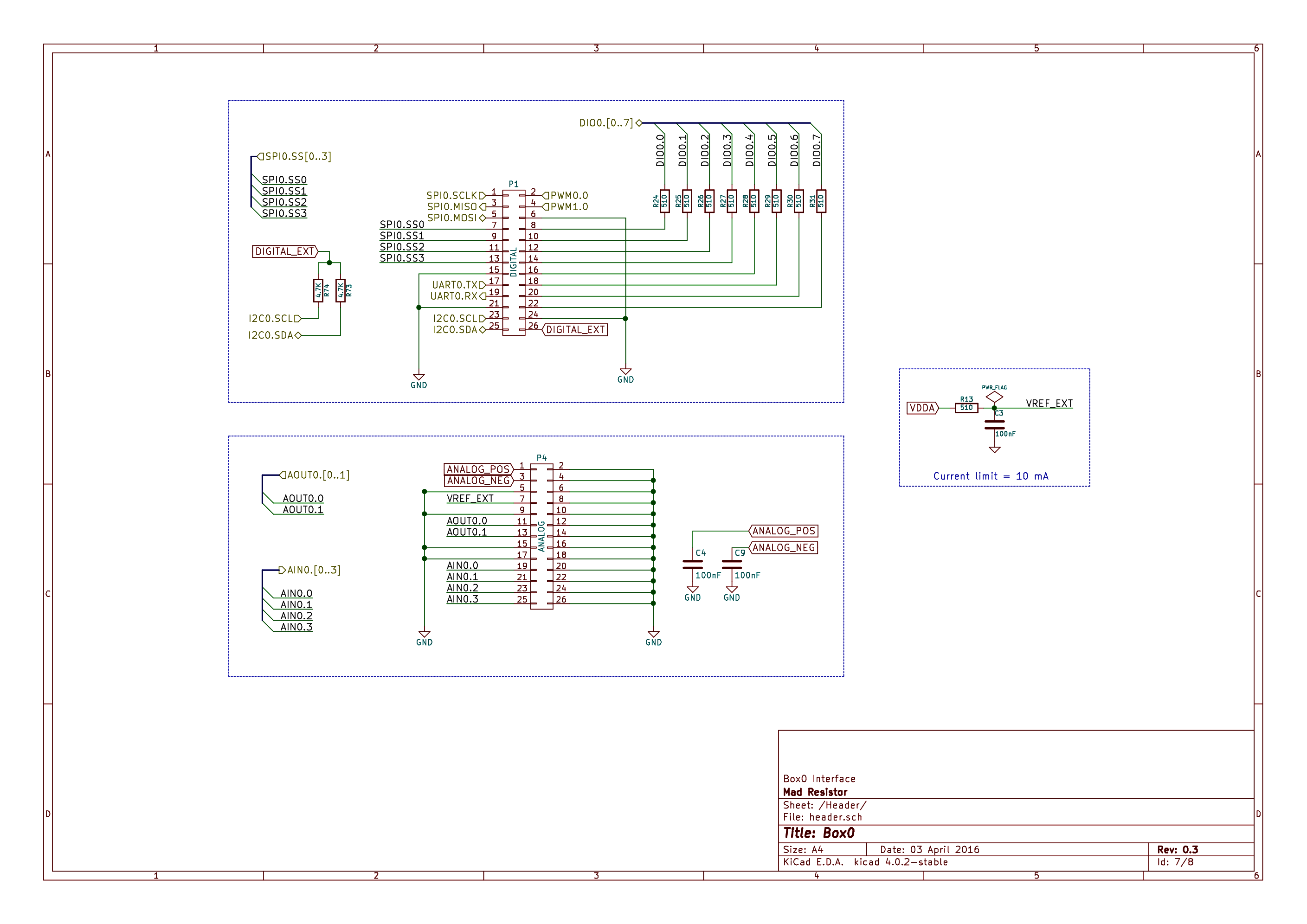
The pin headers for interfacing box0-v5 compatible shields.
- Current limiting resistance for microcontroller pin (as "DIO0" pins).
- I2C bus pull-up
- Current limit resistance for voltage precision reference ("VREF" pin)
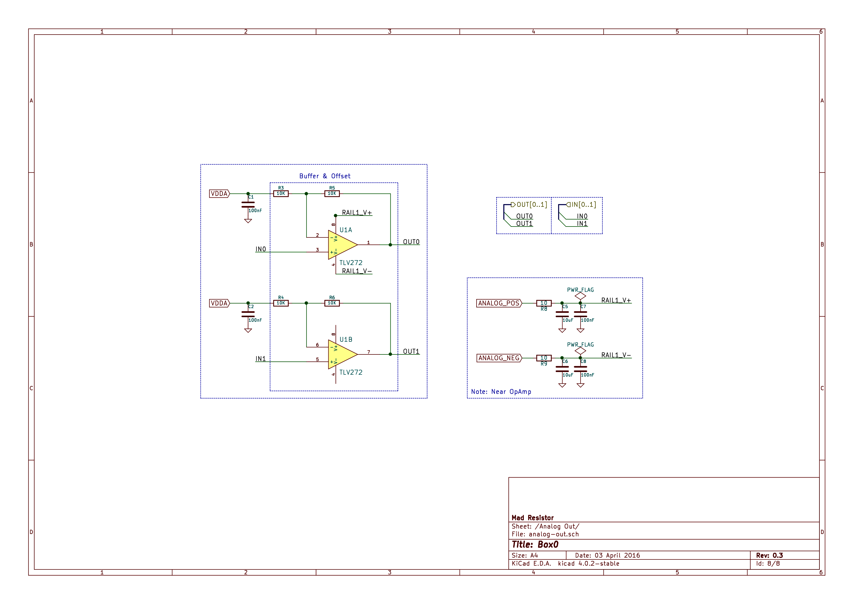
Analog output subsheet.
Aim: Convert 0V to 3.3V to -3.3V to +3.3V.
basically: Offset -> Buffer.
The opamps used is TLV272 in a SOIC8 package which works well for heat dissipaition from the amplifers.These Opamps have in impedance CMOS inputs, low input offset voltage and good output drive capability(much better than the generic jellybean - LM358).
This document be updated in future with more details when we will have some free time.
Discussions
Become a Hackaday.io Member
Create an account to leave a comment. Already have an account? Log In.